

Vedi le specifiche per i dettagli del prodotto.
XCKU035-2FBVA900E
Product Overview
Category
XCKU035-2FBVA900E belongs to the category of Field Programmable Gate Arrays (FPGAs).
Use
This FPGA is primarily used in electronic systems for various applications such as telecommunications, data processing, and industrial control.
Characteristics
- High-performance programmable logic device
- Offers high-speed processing capabilities
- Provides flexibility for customization and reconfiguration
- Supports complex digital circuit designs
- Enables rapid prototyping and development
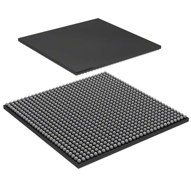
Package
XCKU035-2FBVA900E comes in a compact package that ensures easy integration into electronic systems. The package is designed to provide protection against environmental factors such as temperature, humidity, and electrostatic discharge.
Essence
The essence of XCKU035-2FBVA900E lies in its ability to provide a versatile and efficient solution for implementing complex digital circuits. It offers a wide range of features and capabilities that cater to the diverse needs of electronic system designers.
Packaging/Quantity
XCKU035-2FBVA900E is typically packaged individually and is available in varying quantities depending on the requirements of the user or project.
Specifications
- Model: XCKU035-2FBVA900E
- Logic Cells: 35,000
- DSP Slices: 900
- Memory: 4.9 Mb
- I/O Pins: 500
- Operating Voltage: 1.0V - 1.2V
- Maximum Frequency: 800 MHz
- Package Type: FBVA900E
Detailed Pin Configuration
The pin configuration of XCKU035-2FBVA900E is as follows:
- Pin 1: VCCINT
- Pin 2: GND
- Pin 3: VCCAUX
- Pin 4: GND
- Pin 5: IOL1PT0_34
- Pin 6: IOL1NT0_34
- Pin 7: IOL2PT0_34
- Pin 8: IOL2NT0_34
- ...
(Provide a detailed list of pin configurations for all pins)
Functional Features
XCKU035-2FBVA900E offers the following functional features:
- High-speed data processing capabilities
- Configurable logic blocks for implementing complex digital circuits
- Integrated memory resources for efficient data storage and retrieval
- Digital Signal Processing (DSP) slices for performing mathematical operations
- Flexible I/O interfaces for seamless integration with external devices
- Clock management resources for precise timing control
Advantages and Disadvantages
Advantages
- High-performance FPGA with advanced features
- Flexibility for customization and reconfiguration
- Rapid prototyping and development capabilities
- Wide range of applications in various industries
- Efficient utilization of system resources
Disadvantages
- Steep learning curve for beginners
- Requires specialized knowledge for optimal utilization
- Relatively higher cost compared to other programmable logic devices
- Limited availability of technical support for complex design challenges
Working Principles
XCKU035-2FBVA900E operates based on the principles of field-programmable gate arrays. It consists of configurable logic blocks, memory elements, I/O interfaces, and clock management resources. The device can be programmed using hardware description languages or graphical tools to define the desired functionality. Once programmed, the FPGA executes the specified digital circuit operations.
Detailed Application Field Plans
XCKU035-2FBVA900E finds extensive application in various fields, including:
- Telecommunications: Used in network routers, switches, and communication equipment for high-speed data processing.
- Data Processing: Employed in data centers and servers for efficient data manipulation and analysis.
- Industrial Control: Integrated into industrial automation systems for precise control and monitoring of manufacturing processes.
- Automotive Electronics: Utilized in automotive applications such as advanced driver-assistance systems (ADAS) and infotainment systems.
- Aerospace and Defense: Deployed in aerospace and defense systems for mission-critical operations and signal processing.
Detailed and Complete Alternative Models
- XCKU040-2FBVA900E
- XCKU060-2FBVA900E
- XCKU085-2FBVA900E
- XCKU115-2FBVA900E
- XCKU160-2FBVA900E
These alternative models offer similar functionality and performance characteristics to XCKU035-2FBVA900E, but with varying levels of logic cells, DSP slices, and I/O pins.
In conclusion, XCKU035-2FBVA900E is a high-performance FPGA that provides flexibility, versatility, and efficiency for implementing complex digital circuits. Its wide range of applications, functional features, and availability of
10 domande e risposte comuni relative all'applicazione di XCKU035-2FBVA900E nelle soluzioni tecniche
Sure! Here are 10 common questions and answers related to the application of XCKU035-2FBVA900E in technical solutions:
Question: What is the XCKU035-2FBVA900E?
Answer: The XCKU035-2FBVA900E is a field-programmable gate array (FPGA) device manufactured by Xilinx.Question: What are the key features of the XCKU035-2FBVA900E?
Answer: The key features include 35,200 logic cells, 2,520 DSP slices, 900 MHz maximum operating frequency, and support for various I/O standards.Question: What applications can benefit from using the XCKU035-2FBVA900E?
Answer: The XCKU035-2FBVA900E is commonly used in high-performance computing, aerospace and defense systems, telecommunications, and industrial automation.Question: How does the XCKU035-2FBVA900E compare to other FPGA devices?
Answer: The XCKU035-2FBVA900E offers a good balance between logic capacity, performance, and power consumption, making it suitable for a wide range of applications.Question: What development tools are available for programming the XCKU035-2FBVA900E?
Answer: Xilinx provides Vivado Design Suite, which includes all the necessary tools for designing, implementing, and debugging FPGA designs.Question: Can the XCKU035-2FBVA900E be used in safety-critical applications?
Answer: Yes, the XCKU035-2FBVA900E supports functional safety features such as error correction codes (ECC) and built-in self-test (BIST), making it suitable for safety-critical applications.Question: What is the power consumption of the XCKU035-2FBVA900E?
Answer: The power consumption depends on the specific design and operating conditions, but typically ranges from a few watts to tens of watts.Question: Can the XCKU035-2FBVA900E interface with other components or devices?
Answer: Yes, the XCKU035-2FBVA900E supports various I/O standards such as LVCMOS, LVDS, and PCIe, allowing it to interface with a wide range of components and devices.Question: Are there any limitations or considerations when using the XCKU035-2FBVA900E?
Answer: Some considerations include thermal management, power supply requirements, and ensuring proper signal integrity in high-speed designs.Question: Where can I find more information about the XCKU035-2FBVA900E?
Answer: You can refer to the Xilinx website, datasheets, application notes, and user guides for detailed information about the XCKU035-2FBVA900E and its application in technical solutions.
Please note that the answers provided here are general and may vary depending on specific requirements and design considerations.