

Vedi le specifiche per i dettagli del prodotto.
XC7VX330T-2FF1761I
Product Overview
Category
The XC7VX330T-2FF1761I belongs to the category of Field-Programmable Gate Arrays (FPGAs).
Use
FPGAs are integrated circuits that can be programmed and reprogrammed to perform various digital functions. The XC7VX330T-2FF1761I is specifically designed for high-performance applications.
Characteristics
- High-performance FPGA with advanced features
- Programmable logic cells and configurable I/Os
- Large capacity for complex designs
- High-speed interfaces for data transfer
- Low power consumption
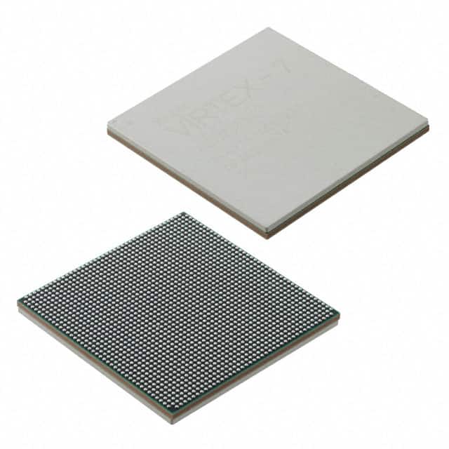
Package
The XC7VX330T-2FF1761I comes in a specific package known as Flip-Chip FineLine BGA (FFBGA). This package offers excellent thermal performance and compact size, making it suitable for space-constrained applications.
Essence
The essence of the XC7VX330T-2FF1761I lies in its ability to provide flexible and customizable digital logic functions. It allows designers to implement complex algorithms and processing tasks efficiently.
Packaging/Quantity
The XC7VX330T-2FF1761I is typically packaged individually and is available in various quantities depending on the manufacturer's specifications.
Specifications
- FPGA Family: Virtex-7
- Logic Cells: 329,200
- CLB Flip-Flops: 1,316,800
- DSP Slices: 3,600
- Block RAM: 36 Mb
- Maximum I/O Count: 1,761
- Operating Voltage: 1.0V
- Operating Temperature Range: -40°C to +100°C
Detailed Pin Configuration
The XC7VX330T-2FF1761I has a comprehensive pin configuration, including input/output pins, power supply pins, and configuration pins. For a detailed pinout diagram and description, please refer to the manufacturer's datasheet.
Functional Features
- High-speed serial transceivers for high-bandwidth data communication
- Integrated memory blocks for efficient data storage and retrieval
- Flexible clock management resources for precise timing control
- Configurable I/O standards to interface with various external devices
- On-chip analog-to-digital converters (ADCs) for sensor integration
- Built-in error correction codes (ECC) for reliable data transmission
Advantages and Disadvantages
Advantages
- Versatile and customizable digital logic functions
- High-performance capabilities for demanding applications
- Low power consumption compared to traditional ASIC designs
- Rapid prototyping and development cycles
- Ability to reconfigure and update functionality without hardware changes
Disadvantages
- Higher cost compared to general-purpose microcontrollers
- Steeper learning curve for FPGA programming and design
- Limited availability of specialized technical support
- Increased complexity in debugging and troubleshooting
Working Principles
The XC7VX330T-2FF1761I operates based on the principles of reconfigurable computing. It consists of programmable logic cells interconnected through configurable routing resources. The device can be programmed using Hardware Description Languages (HDLs) such as VHDL or Verilog. Once programmed, the FPGA executes the desired digital logic functions by routing signals through the configured interconnections.
Detailed Application Field Plans
The XC7VX330T-2FF1761I finds applications in various fields that require high-performance digital processing. Some potential application areas include:
- Telecommunications: Implementing advanced signal processing algorithms for wireless communication systems.
- Aerospace and Defense: Performing real-time image and video processing tasks in radar and surveillance systems.
- High-Performance Computing: Accelerating complex computations in scientific simulations and data analysis.
- Industrial Automation: Controlling and monitoring complex manufacturing processes with high-speed I/O interfaces.
- Medical Imaging: Processing and analyzing medical images for diagnostic purposes.
Detailed and Complete Alternative Models
- XC7VX485T-2FFG1761C: A higher-capacity FPGA from the same Virtex-7 family, offering 484,240 logic cells and 4,840 DSP slices.
- XC7VX690T-2FFG1761I: An even larger FPGA with 686,400 logic cells and 6,840 DSP slices, suitable for extremely demanding applications.
- XC7VX980T-2FFG1761E: The highest-capacity FPGA in the Virtex-7 family, featuring 977,760 logic cells and 9,760 DSP slices.
These alternative models provide increased capacity and performance options for designers with specific requirements.
Note: The above information is based on the specifications available at the time of writing. Please refer to the manufacturer's documentation for the most up-to-date details.
10 domande e risposte comuni relative all'applicazione di XC7VX330T-2FF1761I nelle soluzioni tecniche
Sure! Here are 10 common questions and answers related to the application of XC7VX330T-2FF1761I in technical solutions:
Q1: What is XC7VX330T-2FF1761I? A1: XC7VX330T-2FF1761I is a specific model of Xilinx Virtex-7 FPGA (Field-Programmable Gate Array) with 330,000 logic cells and various features for high-performance applications.
Q2: What are the key features of XC7VX330T-2FF1761I? A2: Some key features include a high-density programmable logic fabric, high-speed serial transceivers, embedded memory blocks, DSP slices, and support for various I/O standards.
Q3: What are the typical applications of XC7VX330T-2FF1761I? A3: XC7VX330T-2FF1761I is commonly used in applications such as wireless communication systems, video processing, radar systems, medical imaging, aerospace, and defense.
Q4: How can XC7VX330T-2FF1761I be programmed? A4: XC7VX330T-2FF1761I can be programmed using Xilinx's Vivado Design Suite, which provides a comprehensive development environment for designing, implementing, and debugging FPGA-based solutions.
Q5: What is the power consumption of XC7VX330T-2FF1761I? A5: The power consumption of XC7VX330T-2FF1761I depends on the specific configuration and operating conditions. It is recommended to refer to the datasheet or use Xilinx's Power Estimator tool for accurate power estimation.
Q6: Can XC7VX330T-2FF1761I be used in safety-critical applications? A6: Yes, XC7VX330T-2FF1761I can be used in safety-critical applications. However, additional measures such as redundancy, fault tolerance, and thorough verification are typically required to ensure the reliability of the overall system.
Q7: What is the maximum operating frequency of XC7VX330T-2FF1761I? A7: The maximum operating frequency of XC7VX330T-2FF1761I depends on the specific design and implementation. It is recommended to perform timing analysis using Xilinx's tools to determine the achievable clock frequency.
Q8: Can XC7VX330T-2FF1761I interface with other components or devices? A8: Yes, XC7VX330T-2FF1761I supports various interfaces such as PCIe, Ethernet, USB, DDR3/DDR4 memory, HDMI, and more. It can be easily integrated into systems that require communication with other components or devices.
Q9: Are there any development boards available for XC7VX330T-2FF1761I? A9: Yes, Xilinx offers development boards like the VC707 and VC709 that feature XC7VX330T-2FF1761I. These boards provide a platform for prototyping and evaluating designs based on this FPGA.
Q10: Can XC7VX330T-2FF1761I be used for real-time signal processing? A10: Yes, XC7VX330T-2FF1761I is well-suited for real-time signal processing applications due to its high-performance capabilities, DSP slices, and support for high-speed serial transceivers. It can handle complex algorithms and data processing tasks efficiently.
Please note that the answers provided here are general and may vary depending on specific design requirements and implementation details.