

Vedi le specifiche per i dettagli del prodotto.
XC7S25-1FTGB196I
Product Overview
Category
XC7S25-1FTGB196I belongs to the category of Field Programmable Gate Arrays (FPGAs).
Use
This product is primarily used in digital logic circuits, where it provides a flexible and customizable solution for implementing complex digital systems.
Characteristics
- High-performance FPGA with advanced features
- Configurable logic blocks and programmable interconnects
- Large number of I/O pins for interfacing with external devices
- Support for various communication protocols
- On-chip memory resources for data storage
- Low power consumption
- Easy reprogrammability
Package
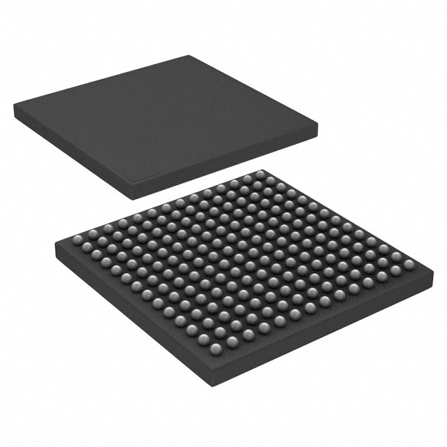
XC7S25-1FTGB196I is available in a 196-ball Fine-Pitch Ball Grid Array (FBGA) package.
Essence
The essence of XC7S25-1FTGB196I lies in its ability to provide a versatile platform for designing and implementing digital circuits. It offers a high level of customization and flexibility, making it suitable for a wide range of applications.
Packaging/Quantity
XC7S25-1FTGB196I is typically sold individually or in small quantities, depending on the requirements of the customer.
Specifications
- FPGA Family: Xilinx 7 Series
- Logic Cells: 24,640
- Look-Up Tables (LUTs): 15,400
- Flip-Flops: 30,800
- Block RAM: 1,620 Kb
- DSP Slices: 80
- Maximum Frequency: 550 MHz
- Operating Voltage: 1.2V
- Temperature Range: -40°C to +100°C
Detailed Pin Configuration
The detailed pin configuration of XC7S25-1FTGB196I can be found in the product datasheet provided by the manufacturer. It includes information about the I/O pins, power supply pins, configuration pins, and other relevant details.
Functional Features
XC7S25-1FTGB196I offers several functional features that enhance its usability and performance:
- Configurable Logic Blocks (CLBs): These blocks consist of Look-Up Tables (LUTs) and Flip-Flops, allowing users to implement custom logic functions.
- Programmable Interconnects: The FPGA provides a flexible interconnection network, enabling efficient communication between different logic elements.
- On-Chip Memory Resources: XC7S25-1FTGB196I includes Block RAMs, which can be used for data storage or as FIFO buffers.
- DSP Slices: Dedicated Digital Signal Processing (DSP) slices provide hardware acceleration for computationally intensive tasks.
- Communication Protocols: The FPGA supports various communication protocols such as UART, SPI, I2C, and Ethernet, facilitating seamless integration with external devices.
Advantages and Disadvantages
Advantages
- High level of customization and flexibility
- Fast development time due to reprogrammability
- Ability to implement complex digital systems on a single chip
- Support for various communication protocols
- Low power consumption compared to traditional ASIC designs
Disadvantages
- Higher cost compared to fixed-function integrated circuits
- Limited resources and scalability compared to larger FPGAs
- Steeper learning curve for beginners due to the complexity of FPGA design
Working Principles
XC7S25-1FTGB196I operates based on the principles of configurable logic and programmable interconnects. The FPGA is programmed using a Hardware Description Language (HDL), such as VHDL or Verilog, which describes the desired functionality of the circuit. The HDL code is then synthesized and mapped onto the FPGA, configuring the logic cells and interconnects accordingly. Once programmed, the FPGA executes the desired digital circuit by routing signals through the configured logic elements.
Detailed Application Field Plans
XC7S25-1FTGB196I finds applications in various fields, including:
- Communications: Used in wireless base stations, routers, and network switches for signal processing and protocol handling.
- Industrial Automation: Employed in control systems, motor drives, and robotics for real-time control and monitoring.
- Aerospace and Defense: Utilized in radar systems, avionics, and secure communication systems for high-performance signal processing.
- Medical Devices: Integrated into medical imaging equipment, patient monitoring systems, and laboratory instruments for data acquisition and processing.
- Automotive: Applied in advanced driver-assistance systems (ADAS), infotainment systems, and engine control units for enhanced functionality and performance.
Alternative Models
For those seeking alternative options, the following FPGA models can be considered:
- XC7A50T-1CSG324C
- XC7K160T-1FBG676I
- XC7Z010-1CLG400C
- XC7VX690T-2FFG176
10 domande e risposte comuni relative all'applicazione di XC7S25-1FTGB196I nelle soluzioni tecniche
Sure! Here are 10 common questions and answers related to the application of XC7S25-1FTGB196I in technical solutions:
Q1: What is XC7S25-1FTGB196I? A1: XC7S25-1FTGB196I is a specific model of Xilinx Spartan-7 FPGA (Field-Programmable Gate Array) that offers high-performance processing capabilities for various technical applications.
Q2: What are the key features of XC7S25-1FTGB196I? A2: Some key features of XC7S25-1FTGB196I include 25,440 logic cells, 1,620 Kbits of block RAM, 90 DSP slices, and support for various I/O standards.
Q3: What are the typical applications of XC7S25-1FTGB196I? A3: XC7S25-1FTGB196I can be used in a wide range of applications such as industrial automation, automotive electronics, telecommunications, medical devices, and more.
Q4: How can XC7S25-1FTGB196I be programmed? A4: XC7S25-1FTGB196I can be programmed using Xilinx's Vivado Design Suite, which provides a comprehensive development environment for FPGA designs.
Q5: What are the power requirements for XC7S25-1FTGB196I? A5: XC7S25-1FTGB196I typically operates at a voltage range of 0.95V to 1.05V and requires a stable power supply with appropriate current capabilities.
Q6: Can XC7S25-1FTGB196I interface with other components or devices? A6: Yes, XC7S25-1FTGB196I supports various communication protocols such as SPI, I2C, UART, and GPIO, allowing it to interface with other components or devices in a system.
Q7: What are the temperature specifications for XC7S25-1FTGB196I? A7: XC7S25-1FTGB196I has an operating temperature range of -40°C to +100°C, making it suitable for both industrial and commercial applications.
Q8: Can XC7S25-1FTGB196I be used for real-time signal processing? A8: Yes, XC7S25-1FTGB196I's high-performance DSP slices make it well-suited for real-time signal processing tasks such as image and video processing, audio processing, and more.
Q9: Is XC7S25-1FTGB196I compatible with other Xilinx FPGA families? A9: XC7S25-1FTGB196I belongs to the Spartan-7 FPGA family, and it is compatible with other members of the same family, allowing for scalability and easy migration between different models.
Q10: Where can I find additional resources and support for XC7S25-1FTGB196I? A10: Xilinx provides comprehensive documentation, application notes, reference designs, and technical support through their website and community forums for XC7S25-1FTGB196I and other FPGA products.
Please note that the answers provided here are general and may vary depending on specific requirements and use cases.