

Vedi le specifiche per i dettagli del prodotto.
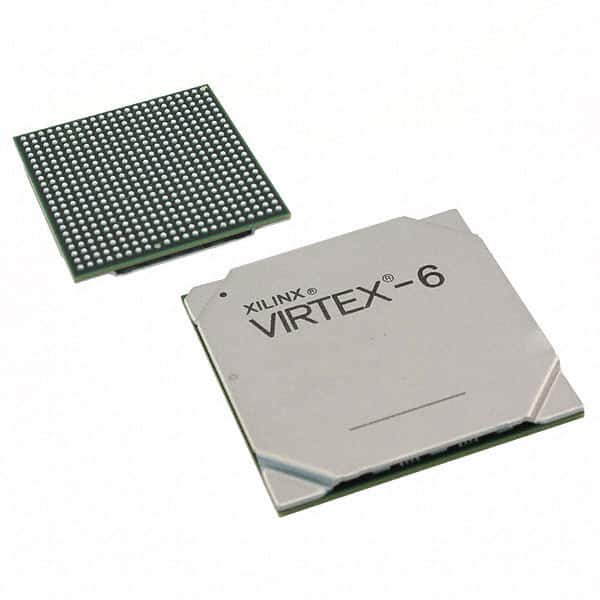
XC6VLX240T-L1FFG1759I
Basic Information Overview
- Category: Field Programmable Gate Array (FPGA)
- Use: Digital logic implementation, prototyping, and system integration
- Characteristics:
- High-performance programmable logic device
- Large capacity with 240,000 logic cells
- Advanced process technology for improved speed and power efficiency
- Flexible I/O options for interfacing with external devices
- Package: Flip-chip BGA (Ball Grid Array)
- Essence: Versatile and reconfigurable integrated circuit for custom digital designs
- Packaging/Quantity: Available in trays or reels, quantity depends on customer requirements
Specifications
- Logic Cells: 240,000
- Slices: 15,360
- DSP48E1 Slices: 768
- Block RAM: 4,860 Kb
- Maximum Frequency: 550 MHz
- I/O Pins: 800
- Operating Voltage: 1.0V - 1.2V
- Operating Temperature: -40°C to +100°C
Detailed Pin Configuration
- The XC6VLX240T-L1FFG1759I has a complex pin configuration with various pins dedicated to different functions. For a detailed pinout diagram and description, please refer to the manufacturer's datasheet.
Functional Features
- High-performance FPGA with advanced architecture
- Configurable logic cells for implementing complex digital designs
- Dedicated DSP slices for efficient signal processing
- Flexible I/O options for interfacing with various external devices
- On-chip memory blocks for data storage and retrieval
- Built-in clock management resources for precise timing control
- Support for various communication protocols and standards
Advantages
- Versatility: Can be programmed and reconfigured for different applications
- Scalability: Offers a wide range of logic capacity options
- Speed: High-performance architecture enables fast processing
- Integration: Can integrate multiple functions into a single device
- Flexibility: Supports various I/O standards and interfaces
Disadvantages
- Complexity: Requires expertise in FPGA design and programming
- Power Consumption: Large FPGAs can consume significant power
- Cost: Higher cost compared to fixed-function integrated circuits
- Development Time: Designing and implementing FPGA-based systems can be time-consuming
Working Principles
- The XC6VLX240T-L1FFG1759I is based on the principle of reconfigurable logic. It consists of an array of configurable logic cells that can be programmed to implement desired digital logic functions. These logic cells are interconnected through programmable routing resources, allowing for flexible interconnection between different components. The FPGA can be programmed using hardware description languages (HDL) or graphical tools, which define the desired functionality and interconnections. Once programmed, the FPGA operates as a custom digital circuit, executing the specified logic operations.
Detailed Application Field Plans
- The XC6VLX240T-L1FFG1759I finds applications in various fields, including:
- Telecommunications: Used in base stations, network routers, and communication equipment for signal processing and protocol handling.
- Aerospace and Defense: Employed in radar systems, avionics, and military communication systems for high-speed data processing and control.
- Industrial Automation: Utilized in control systems, robotics, and factory automation for real-time data processing and control.
- Medical Devices: Integrated into medical imaging systems, patient monitoring devices, and diagnostic equipment for signal processing and data analysis.
- Automotive: Used in advanced driver-assistance systems (ADAS), infotainment systems, and engine control units (ECUs) for processing sensor data and controlling vehicle functions.
Detailed and Complete Alternative Models
- Alternative models with similar capabilities and features to the XC6VLX240T-L1FFG1759I include:
- Xilinx Virtex-7 Series FPGAs
- Intel (Altera) Stratix V Series FPGAs
- Lattice Semiconductor ECP5 Series FPGAs
- Microsemi (Microchip) SmartFusion2 Series FPGAs
Note: The above information is a general overview of the XC6VLX240T-L1FFG1759I FPGA. For detailed technical specifications, pin configurations, and application-specific considerations, please refer to the manufacturer's datasheet and documentation.
Word Count: 496
10 domande e risposte comuni relative all'applicazione di XC6VLX240T-L1FFG1759I nelle soluzioni tecniche
Sure! Here are 10 common questions and answers related to the application of XC6VLX240T-L1FFG1759I in technical solutions:
Q1: What is XC6VLX240T-L1FFG1759I? A1: XC6VLX240T-L1FFG1759I is a field-programmable gate array (FPGA) manufactured by Xilinx. It is part of the Virtex-6 family and offers high-performance capabilities for various applications.
Q2: What are the key features of XC6VLX240T-L1FFG1759I? A2: Some key features of XC6VLX240T-L1FFG1759I include a large number of logic cells, high-speed serial transceivers, embedded memory blocks, DSP slices, and support for various communication protocols.
Q3: What are the typical applications of XC6VLX240T-L1FFG1759I? A3: XC6VLX240T-L1FFG1759I can be used in a wide range of applications such as telecommunications, aerospace, defense, industrial automation, medical imaging, video processing, and scientific research.
Q4: How can XC6VLX240T-L1FFG1759I be programmed? A4: XC6VLX240T-L1FFG1759I can be programmed using Xilinx's Vivado Design Suite or ISE Design Suite. These software tools provide a graphical interface and HDL-based design flow to program the FPGA.
Q5: What is the maximum operating frequency of XC6VLX240T-L1FFG1759I? A5: The maximum operating frequency of XC6VLX240T-L1FFG1759I depends on the specific design and implementation. However, it is capable of operating at high frequencies, typically in the range of hundreds of megahertz to several gigahertz.
Q6: Can XC6VLX240T-L1FFG1759I interface with other components or devices? A6: Yes, XC6VLX240T-L1FFG1759I supports various communication protocols such as PCIe, Ethernet, USB, SPI, I2C, and more. It can interface with other components or devices through these protocols.
Q7: Does XC6VLX240T-L1FFG1759I have built-in memory? A7: Yes, XC6VLX240T-L1FFG1759I has embedded memory blocks (BRAM) that can be used for storing data or implementing memory-intensive functions in the FPGA design.
Q8: What is the power consumption of XC6VLX240T-L1FFG1759I? A8: The power consumption of XC6VLX240T-L1FFG1759I depends on the specific design and utilization. It is recommended to refer to the datasheet and power estimation tools provided by Xilinx for accurate power analysis.
Q9: Can XC6VLX240T-L1FFG1759I be used in safety-critical applications? A9: Yes, XC6VLX240T-L1FFG1759I can be used in safety-critical applications. However, it is important to follow appropriate design practices, perform thorough testing, and ensure compliance with relevant safety standards.
Q10: Are there any development boards or evaluation kits available for XC6VLX240T-L1FFG1759I? A10: Yes, Xilinx offers development boards and evaluation kits specifically designed for XC6VLX240T-L1FFG1759I. These kits provide a platform for prototyping and testing FPGA designs using the specific device.