

Vedi le specifiche per i dettagli del prodotto.
XC4VLX100-10FFG1148I
Product Overview
Category
The XC4VLX100-10FFG1148I belongs to the category of Field Programmable Gate Arrays (FPGAs).
Use
FPGAs are integrated circuits that can be programmed and reprogrammed to perform various digital functions. The XC4VLX100-10FFG1148I is specifically designed for high-performance applications that require complex logic functions.
Characteristics
- High-performance FPGA with advanced features
- Large capacity for complex designs
- Flexible and reprogrammable
- Low power consumption
- High-speed data processing capabilities
Package
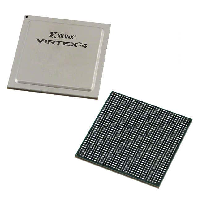
The XC4VLX100-10FFG1148I comes in a specific package known as FFG1148, which refers to the Fine-Pitch Ball Grid Array (FBGA) package with 1148 balls.
Essence
The essence of the XC4VLX100-10FFG1148I lies in its ability to provide a versatile and powerful platform for implementing complex digital designs.
Packaging/Quantity
The XC4VLX100-10FFG1148I is typically sold individually or in small quantities, depending on the supplier's packaging options.
Specifications
- Logic Cells: 100,000
- Flip-Flops: 64,000
- Block RAM: 1,728 Kbits
- DSP Slices: 192
- Maximum Frequency: 500 MHz
- I/O Pins: 648
- Operating Voltage: 1.2V
Detailed Pin Configuration
The XC4VLX100-10FFG1148I has a total of 648 I/O pins, each serving a specific purpose in the overall functionality of the FPGA. A detailed pin configuration diagram can be found in the product datasheet.
Functional Features
- High-speed data processing capabilities
- Configurable logic blocks for flexible design implementation
- Dedicated DSP slices for efficient signal processing
- Abundant memory resources for data storage and retrieval
- Built-in clock management resources for precise timing control
Advantages and Disadvantages
Advantages
- Versatile and reprogrammable platform for complex digital designs
- High-performance capabilities suitable for demanding applications
- Low power consumption compared to alternative solutions
- Abundant I/O pins for interfacing with external devices
- Extensive support and development tools available from the manufacturer
Disadvantages
- Higher cost compared to traditional fixed-function integrated circuits
- Steeper learning curve for beginners due to the complexity of FPGA programming
- Limited availability of alternative models with similar specifications
Working Principles
The XC4VLX100-10FFG1148I operates based on the principles of configurable logic. It consists of a matrix of programmable logic cells interconnected by configurable routing resources. The user can program the FPGA to implement desired logic functions by configuring the interconnections between the logic cells.
Detailed Application Field Plans
The XC4VLX100-10FFG1148I finds applications in various fields, including: 1. Telecommunications: High-speed data processing and protocol handling. 2. Aerospace and Defense: Radar and signal processing, encryption, and secure communication systems. 3. Industrial Automation: Control systems, motor control, and real-time monitoring. 4. Medical Devices: Image processing, diagnostics, and patient monitoring. 5. Automotive: Advanced driver assistance systems (ADAS), infotainment, and engine control.
Detailed and Complete Alternative Models
While the XC4VLX100-10FFG1148I offers a unique combination of features, there are alternative FPGA models available with similar capabilities. Some notable alternatives include: - Xilinx Virtex-7 series - Intel (formerly Altera) Stratix series - Lattice Semiconductor ECP5 series
These alternative models provide a range of options for designers based on specific requirements and preferences.
Word count: 511
10 domande e risposte comuni relative all'applicazione di XC4VLX100-10FFG1148I nelle soluzioni tecniche
Sure! Here are 10 common questions and answers related to the application of XC4VLX100-10FFG1148I in technical solutions:
Q: What is XC4VLX100-10FFG1148I? A: XC4VLX100-10FFG1148I is a field-programmable gate array (FPGA) from Xilinx, which offers high-performance logic and signal processing capabilities.
Q: What are the key features of XC4VLX100-10FFG1148I? A: Some key features include 100,000 logic cells, 10ns minimum clock period, 1.2V core voltage, and 1.5V/2.5V/3.3V I/O standards support.
Q: What are the typical applications of XC4VLX100-10FFG1148I? A: XC4VLX100-10FFG1148I is commonly used in applications such as telecommunications, networking, industrial automation, aerospace, and defense.
Q: How can XC4VLX100-10FFG1148I be programmed? A: XC4VLX100-10FFG1148I can be programmed using Xilinx's Vivado Design Suite or ISE Design Suite software tools.
Q: What is the maximum operating frequency of XC4VLX100-10FFG1148I? A: The maximum operating frequency of XC4VLX100-10FFG1148I is 100 MHz.
Q: Can XC4VLX100-10FFG1148I interface with other devices? A: Yes, XC4VLX100-10FFG1148I supports various interfaces such as PCIe, Ethernet, USB, SPI, I2C, and UART.
Q: What is the power consumption of XC4VLX100-10FFG1148I? A: The power consumption of XC4VLX100-10FFG1148I depends on the design and utilization, but it typically ranges from 1W to 5W.
Q: Can XC4VLX100-10FFG1148I be used for real-time signal processing? A: Yes, XC4VLX100-10FFG1148I is capable of real-time signal processing due to its high-performance capabilities and low-latency architecture.
Q: Does XC4VLX100-10FFG1148I support partial reconfiguration? A: No, XC4VLX100-10FFG1148I does not support partial reconfiguration. It requires a full bitstream reload for any design changes.
Q: Are there any development boards available for XC4VLX100-10FFG1148I? A: Yes, Xilinx offers development boards like the ML403 or ML410 that are compatible with XC4VLX100-10FFG1148I for prototyping and evaluation purposes.
Please note that the answers provided here are general and may vary depending on specific requirements and use cases.