

Vedi le specifiche per i dettagli del prodotto.
XC4062XL-1HQ304I
Product Overview
Category
The XC4062XL-1HQ304I belongs to the category of programmable logic devices (PLDs).
Use
This product is primarily used in digital circuit design and implementation. It offers a flexible and customizable solution for various applications.
Characteristics
- Programmable: The XC4062XL-1HQ304I can be programmed to perform specific functions based on user requirements.
- High-density: It provides a high number of logic elements, allowing for complex designs.
- Low power consumption: The device is designed to operate efficiently with minimal power consumption.
- Fast operation: The XC4062XL-1HQ304I offers high-speed performance, enabling rapid data processing.
Package
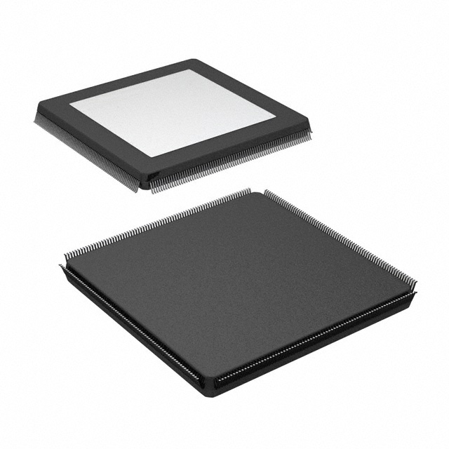
The XC4062XL-1HQ304I is available in a compact quad flat pack (QFP) package.
Essence
The essence of this product lies in its ability to provide reconfigurable logic functionality, allowing designers to implement custom digital circuits without the need for dedicated hardware.
Packaging/Quantity
The XC4062XL-1HQ304I is typically packaged in reels or trays, with each containing a specified quantity of devices.
Specifications
- Device type: Programmable Logic Device (PLD)
- Family: XC4000XL
- Logic cells: 62,000
- I/O pins: 304
- Operating voltage: 3.3V
- Speed grade: -1HQ
- Package type: Quad Flat Pack (QFP)
Detailed Pin Configuration
The XC4062XL-1HQ304I has a total of 304 I/O pins, which are organized into different banks. Each pin serves a specific purpose and can be configured as an input or output based on the desired functionality.
For a detailed pin configuration diagram, please refer to the datasheet provided by the manufacturer.
Functional Features
- Reconfigurable logic: The XC4062XL-1HQ304I allows users to modify the functionality of the device even after it has been programmed, providing flexibility in design.
- High-speed performance: This PLD offers fast operation, making it suitable for applications that require quick data processing.
- Versatile I/O capabilities: With 304 I/O pins, the XC4062XL-1HQ304I provides ample connectivity options for interfacing with external devices.
- Low power consumption: The device is designed to operate efficiently, minimizing power consumption and reducing overall system energy requirements.
Advantages and Disadvantages
Advantages
- Flexibility in design due to reconfigurable logic
- High-density logic elements for complex designs
- Fast operation for rapid data processing
- Versatile I/O capabilities for interfacing with external devices
Disadvantages
- Limited availability of I/O pins compared to larger PLDs
- Higher cost compared to simpler programmable devices
Working Principles
The XC4062XL-1HQ304I operates based on the principles of programmable logic. It consists of a matrix of configurable logic blocks (CLBs) interconnected through programmable interconnects. These CLBs can be configured to perform specific logic functions, allowing designers to implement custom digital circuits.
The device is programmed using hardware description languages (HDLs) or schematic entry tools. Once programmed, the XC4062XL-1HQ304I executes the desired logic functions, enabling the implementation of various digital circuit designs.
Detailed Application Field Plans
The XC4062XL-1HQ304I finds applications in a wide range of fields, including:
- Communications: Used in networking equipment, routers, and switches for data processing and control.
- Industrial automation: Employed in programmable logic controllers (PLCs) for process control and monitoring.
- Consumer electronics: Integrated into devices such as gaming consoles, set-top boxes, and multimedia systems for custom functionality.
- Automotive: Utilized in automotive control systems for functions like engine management, safety features, and infotainment systems.
- Aerospace: Applied in avionics systems for flight control, navigation, and communication.
Detailed and Complete Alternative Models
- XC4000EX-4PQ160C: A similar PLD with 4,000 logic cells and 160 I/O pins, suitable for smaller-scale designs.
- XC9572XL-10VQG44C: An alternative PLD with 9,572 logic cells and 44 I/O pins, offering a balance between density and cost.
- XC2S100E-6TQ144I: A different PLD with 100,000 system gates and 144 I/O pins, providing higher capacity for complex designs.
These alternative models offer varying specifications and capabilities, allowing designers to choose the most suitable option based on their specific requirements.
Word count: 660 words
10 domande e risposte comuni relative all'applicazione di XC4062XL-1HQ304I nelle soluzioni tecniche
Sure! Here are 10 common questions and answers related to the application of XC4062XL-1HQ304I in technical solutions:
Q1: What is XC4062XL-1HQ304I? A1: XC4062XL-1HQ304I is a field-programmable gate array (FPGA) manufactured by Xilinx. It is a high-density, high-performance device used for implementing digital logic circuits.
Q2: What are the key features of XC4062XL-1HQ304I? A2: Some key features of XC4062XL-1HQ304I include 62,208 logic cells, 3,072 Kbits of block RAM, 192 user I/O pins, and a maximum operating frequency of 200 MHz.
Q3: What are the typical applications of XC4062XL-1HQ304I? A3: XC4062XL-1HQ304I is commonly used in various technical solutions such as telecommunications, industrial automation, aerospace, defense systems, medical equipment, and scientific research.
Q4: How can XC4062XL-1HQ304I be programmed? A4: XC4062XL-1HQ304I can be programmed using Hardware Description Languages (HDLs) like VHDL or Verilog. Xilinx provides software tools like Vivado or ISE Design Suite for designing, simulating, and programming the FPGA.
Q5: Can XC4062XL-1HQ304I be reprogrammed after it has been programmed once? A5: Yes, XC4062XL-1HQ304I is a reprogrammable FPGA. It can be erased and reprogrammed multiple times, allowing for flexibility in design iterations and updates.
Q6: What is the power supply requirement for XC4062XL-1HQ304I? A6: XC4062XL-1HQ304I typically operates at a voltage of 3.3V, but it also supports a wide range of power supply voltages from 2.5V to 5V.
Q7: Can XC4062XL-1HQ304I interface with other components or devices? A7: Yes, XC4062XL-1HQ304I can interface with various components and devices through its user I/O pins. It supports different communication protocols like SPI, I2C, UART, and Ethernet.
Q8: What is the maximum operating frequency of XC4062XL-1HQ304I? A8: The maximum operating frequency of XC4062XL-1HQ304I is 200 MHz. However, the achievable frequency depends on the complexity of the design and the specific implementation.
Q9: Are there any limitations or considerations when using XC4062XL-1HQ304I? A9: Some considerations include power consumption, thermal management, signal integrity, and timing constraints. It is important to carefully analyze and optimize the design to meet these requirements.
Q10: Where can I find additional resources or support for XC4062XL-1HQ304I? A10: Xilinx provides comprehensive documentation, application notes, reference designs, and technical support through their website. Additionally, online forums and communities dedicated to FPGA development can be helpful sources of information.