

Vedi le specifiche per i dettagli del prodotto.
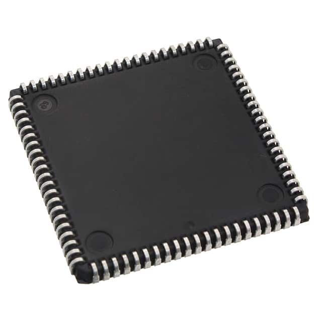
XC4006E-4PC84C
Product Overview
Category
XC4006E-4PC84C belongs to the category of programmable logic devices (PLDs).
Use
This product is used in digital circuit design and implementation. It provides a flexible and customizable solution for various applications.
Characteristics
- Programmable: The XC4006E-4PC84C can be programmed to perform specific functions based on the user's requirements.
- High Integration: It integrates multiple logic gates, flip-flops, and other components into a single device, reducing the need for external components.
- Versatile: It can be used in a wide range of applications, including telecommunications, automotive, industrial control, and consumer electronics.
- Low Power Consumption: The XC4006E-4PC84C is designed to operate efficiently with low power consumption.
- Compact Package: It comes in a PC84C package, which is compact and suitable for space-constrained designs.
Packaging/Quantity
The XC4006E-4PC84C is typically packaged in trays or tubes. The quantity per package varies depending on the manufacturer and distributor.
Specifications
- Logic Cells: 400
- Maximum Frequency: 50 MHz
- Operating Voltage: 3.3V
- I/O Pins: 84
- Operating Temperature Range: -40°C to 85°C
- Package Type: Plastic Quad Flat Pack (PQFP)
Detailed Pin Configuration
The XC4006E-4PC84C has a total of 84 pins. Here is a brief overview of the pin configuration:
- Pin 1: VCCIO
- Pin 2: GND
- Pin 3: IO0
- Pin 4: IO1
- ...
- Pin 83: IO82
- Pin 84: IO83
For a detailed pin configuration diagram, please refer to the product datasheet.
Functional Features
- Programmable Logic: The XC4006E-4PC84C offers a wide range of programmable logic elements, allowing users to implement complex digital circuits.
- I/O Flexibility: It provides 84 I/O pins for interfacing with external devices or other components in the system.
- Clock Management: The device supports clock management features, enabling precise timing control for synchronous operations.
- Embedded Memory: The XC4006E-4PC84C includes embedded memory blocks that can be used for data storage or lookup table implementation.
Advantages and Disadvantages
Advantages
- Flexibility: The programmable nature of XC4006E-4PC84C allows for easy customization and modification of designs.
- Cost-Effective: By eliminating the need for multiple discrete components, it reduces overall system costs.
- Time-to-Market: PLDs like XC4006E-4PC84C enable faster prototyping and development cycles, reducing time-to-market for new products.
Disadvantages
- Limited Complexity: Compared to more advanced programmable devices, the XC4006E-4PC84C has a limited number of logic cells, which may restrict the complexity of designs.
- Learning Curve: Utilizing PLDs requires knowledge of hardware description languages (HDL) and design tools, which may have a learning curve for beginners.
Working Principles
The XC4006E-4PC84C utilizes a combination of programmable logic elements, interconnects, and embedded memory blocks to implement user-defined digital circuits. These circuits are configured by programming the device using specialized software tools. Once programmed, the XC4006E-4PC84C executes the desired functionality based on the programmed logic.
Detailed Application Field Plans
The XC4006E-4PC84C is suitable for various application fields, including:
- Telecommunications: It can be used in communication systems for signal processing, protocol conversion, and data routing.
- Automotive: The XC4006E-4PC84C finds applications in automotive electronics, such as engine control units, infotainment systems, and advanced driver-assistance systems (ADAS).
- Industrial Control: It is utilized in industrial automation for controlling machinery, monitoring sensors, and implementing complex control algorithms.
- Consumer Electronics: The XC4006E-4PC84C can be integrated into consumer electronic devices like gaming consoles, home appliances, and audio/video equipment.
Detailed and Complete Alternative Models
- XC4005E-4PC84C
- XC4008E-4PC84C
- XC4010E-4PC84C
- XC4013E-4PC84C
- XC4016E-4PC84C
These alternative models offer similar functionality and characteristics to the XC4006E-4PC84C, but with varying logic cell counts and I/O pin configurations.
In conclusion, the XC4006E-
10 domande e risposte comuni relative all'applicazione di XC4006E-4PC84C nelle soluzioni tecniche
Sure! Here are 10 common questions and answers related to the application of XC4006E-4PC84C in technical solutions:
Question: What is XC4006E-4PC84C?
Answer: XC4006E-4PC84C is a specific model of Field Programmable Gate Array (FPGA) manufactured by Xilinx.Question: What are the key features of XC4006E-4PC84C?
Answer: Some key features of XC4006E-4PC84C include 4000 gates, 84-pin plastic package, and 4ns maximum pin-to-pin delay.Question: In what applications can XC4006E-4PC84C be used?
Answer: XC4006E-4PC84C can be used in various applications such as digital signal processing, telecommunications, industrial control systems, and automotive electronics.Question: How does XC4006E-4PC84C differ from other FPGAs?
Answer: XC4006E-4PC84C is known for its low power consumption, high performance, and cost-effectiveness compared to other FPGAs in its class.Question: Can XC4006E-4PC84C be reprogrammed after deployment?
Answer: Yes, XC4006E-4PC84C is a field-programmable device, which means it can be reprogrammed even after it has been deployed in a system.Question: What development tools are available for programming XC4006E-4PC84C?
Answer: Xilinx provides software tools like Vivado Design Suite and ISE Design Suite that can be used for programming and configuring XC4006E-4PC84C.Question: What is the maximum operating frequency of XC4006E-4PC84C?
Answer: The maximum operating frequency of XC4006E-4PC84C depends on the specific design and implementation, but it can typically reach frequencies in the range of tens to hundreds of megahertz.Question: Can XC4006E-4PC84C interface with other components or devices?
Answer: Yes, XC4006E-4PC84C supports various communication protocols such as SPI, I2C, UART, and GPIO, allowing it to interface with other components or devices in a system.Question: Are there any limitations or considerations when using XC4006E-4PC84C?
Answer: Some considerations include power supply requirements, thermal management, and ensuring proper signal integrity in high-speed designs.Question: Where can I find more information about XC4006E-4PC84C?
Answer: You can refer to the official Xilinx website, datasheets, application notes, or consult with Xilinx representatives for more detailed information about XC4006E-4PC84C.