

Vedi le specifiche per i dettagli del prodotto.
XC4006E-2PC84I
Product Overview
Category
XC4006E-2PC84I belongs to the category of Field Programmable Gate Arrays (FPGAs).
Use
This product is primarily used in digital circuit design and implementation. FPGAs provide a flexible and customizable solution for various applications, including telecommunications, automotive, aerospace, and consumer electronics.
Characteristics
- Programmable: FPGAs can be reprogrammed to perform different functions, allowing for versatility in design.
- High Performance: XC4006E-2PC84I offers high-speed operation and efficient processing capabilities.
- Integration: This FPGA integrates multiple logic elements, memory blocks, and I/O interfaces on a single chip.
- Configurability: The device can be configured to meet specific application requirements.
Package
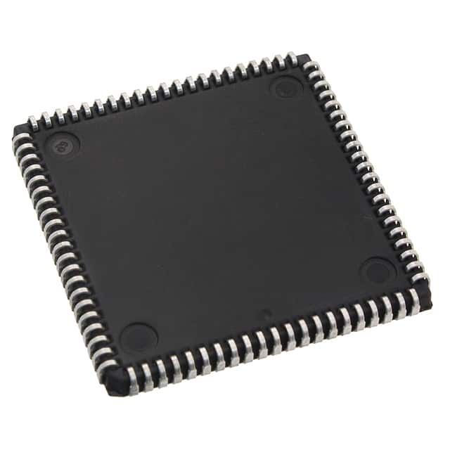
XC4006E-2PC84I is available in a 84-pin plastic quad flat pack (PQFP) package.
Essence
The essence of XC4006E-2PC84I lies in its ability to provide a programmable hardware platform that enables designers to implement complex digital circuits efficiently.
Packaging/Quantity
This product is typically packaged in reels or trays, with a quantity of 250 units per reel/tray.
Specifications
- Logic Cells: 4000
- Maximum Frequency: 100 MHz
- Operating Voltage: 3.3V
- I/O Pins: 68
- Memory Blocks: 64
- Configuration Bits: 6000
- Package Type: PQFP
- Temperature Range: -40°C to +85°C
Detailed Pin Configuration
The pin configuration of XC4006E-2PC84I is as follows:
- VCCIO
- GND
- IOB0
- IOB1
- IOB2
- IOB3
- IOB4
- IOB5
- IOB6
- IOB7
- IOB8
- IOB9
- IOB10
- IOB11
- IOB12
- IOB13
- IOB14
- IOB15
- IOB16
- IOB17
- IOB18
- IOB19
- IOB20
- IOB21
- IOB22
- IOB23
- IOB24
- IOB25
- IOB26
- IOB27
- IOB28
- IOB29
- IOB30
- IOB31
- IOB32
- IOB33
- IOB34
- IOB35
- IOB36
- IOB37
- IOB38
- IOB39
- IOB40
- IOB41
- IOB42
- IOB43
- IOB44
- IOB45
- IOB46
- IOB47
- IOB48
- IOB49
- IOB50
- IOB51
- IOB52
- IOB53
- IOB54
- IOB55
- IOB56
- IOB57
- IOB58
- IOB59
- IOB60
- IOB61
- IOB62
- IOB63
- GND
- VCCIO
Functional Features
XC4006E-2PC84I offers the following functional features:
- Programmable Logic Blocks (PLBs): These blocks provide configurable logic elements that can be interconnected to implement desired digital circuits.
- Input/Output Blocks (IOBs): IOBs facilitate communication between the FPGA and external devices through configurable I/O pins.
- Memory Blocks: The integrated memory blocks offer storage capabilities for data processing and temporary storage requirements.
- Clock Management: XC4006E-2PC84I includes clock management resources, such as phase-locked loops (PLLs), to generate stable clock signals for synchronous operations.
- Configuration Interface: The device supports various configuration interfaces, allowing for easy programming and reconfiguration.
Advantages and Disadvantages
Advantages
- Flexibility: The programmable nature of FPGAs allows for rapid prototyping and design iterations.
- Customizability: XC4006E-2PC84I enables designers to create tailored solutions for specific applications.
- Integration: The integration of multiple components on a single chip reduces the need for additional external components.
- High Performance: FPGAs offer high-speed operation and parallel processing capabilities.
Disadvantages
10 domande e risposte comuni relative all'applicazione di XC4006E-2PC84I nelle soluzioni tecniche
Sure! Here are 10 common questions and answers related to the application of XC4006E-2PC84I in technical solutions:
Q: What is XC4006E-2PC84I? A: XC4006E-2PC84I is a specific model of Field Programmable Gate Array (FPGA) manufactured by Xilinx.
Q: What are the key features of XC4006E-2PC84I? A: Some key features of XC4006E-2PC84I include 4000 gates, 84-pin plastic package, and 5V operation.
Q: What are the typical applications of XC4006E-2PC84I? A: XC4006E-2PC84I can be used in various applications such as digital signal processing, data communication, and control systems.
Q: How does XC4006E-2PC84I differ from other FPGA models? A: XC4006E-2PC84I has a specific gate count, pin configuration, and voltage requirement that differentiate it from other FPGA models.
Q: Can XC4006E-2PC84I be programmed using industry-standard tools? A: Yes, XC4006E-2PC84I can be programmed using Xilinx's Vivado Design Suite or other compatible development tools.
Q: What programming languages can be used with XC4006E-2PC84I? A: XC4006E-2PC84I can be programmed using Hardware Description Languages (HDLs) such as VHDL or Verilog.
Q: Is XC4006E-2PC84I suitable for high-speed applications? A: While XC4006E-2PC84I is capable of operating at high speeds, it is recommended to consult the datasheet and design guidelines for specific requirements.
Q: Can XC4006E-2PC84I be used in low-power applications? A: XC4006E-2PC84I is not specifically designed for low-power applications. Xilinx offers other FPGA models that are more suitable for low-power designs.
Q: Are there any limitations or considerations when using XC4006E-2PC84I? A: Some considerations include power supply requirements, I/O voltage levels, and maximum operating frequency specified in the datasheet.
Q: Where can I find additional resources and support for XC4006E-2PC84I? A: You can refer to Xilinx's official website, user guides, application notes, and online forums for additional resources and support related to XC4006E-2PC84I.
Please note that the answers provided here are general and may vary depending on specific requirements and use cases. It is always recommended to consult the manufacturer's documentation and seek expert advice when working with specific technical solutions.