

Vedi le specifiche per i dettagli del prodotto.
XC3S400-5FGG456C
Product Overview
Category
XC3S400-5FGG456C belongs to the category of Field-Programmable Gate Arrays (FPGAs).
Use
FPGAs are integrated circuits that can be programmed and reprogrammed to perform various digital functions. They are widely used in industries such as telecommunications, automotive, aerospace, and consumer electronics.
Characteristics
XC3S400-5FGG456C is known for its high-performance capabilities, low power consumption, and flexibility in design. It offers a wide range of features and functionalities that make it suitable for complex applications.
Package
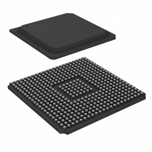
XC3S400-5FGG456C comes in a compact package that ensures easy integration into electronic systems. The package type is FG456, which refers to a fine-pitch grid array with 456 pins.
Essence
The essence of XC3S400-5FGG456C lies in its ability to provide a customizable hardware solution that can be tailored to specific application requirements. Its programmable nature allows for quick prototyping and iterative development.
Packaging/Quantity
XC3S400-5FGG456C is typically packaged in reels or trays, depending on the manufacturer's specifications. The quantity per package may vary, but it is commonly available in quantities suitable for both small-scale and large-scale production.
Specifications
- FPGA Family: Spartan-3
- Logic Cells: 400,000
- Number of I/Os: 456
- Operating Voltage: 1.2V
- Maximum Frequency: 500 MHz
- Embedded Memory: Up to 4.8 Mb
- DSP Slices: 48
- Configuration: In-system programmable (ISP) via JTAG interface
Detailed Pin Configuration
The pin configuration of XC3S400-5FGG456C is as follows:
- Pin 1: VCCIO
- Pin 2: GND
- Pin 3: IOB33
- Pin 4: IOB32
- Pin 5: IOB31
- ...
- Pin 456: GND
For a complete pin configuration diagram, please refer to the datasheet provided by the manufacturer.
Functional Features
XC3S400-5FGG456C offers several functional features that enhance its performance and versatility. Some of these features include:
- High-speed I/O interfaces
- On-chip memory blocks
- Digital Signal Processing (DSP) slices
- Clock Management Tiles (CMT)
- Flexible routing resources
- Built-in self-test capabilities
Advantages and Disadvantages
Advantages
- Flexibility in design and reconfiguration
- High-performance capabilities
- Low power consumption
- Quick prototyping and development
- Wide range of application possibilities
Disadvantages
- Steep learning curve for beginners
- Limited availability of technical support
- Higher cost compared to other programmable logic devices
Working Principles
XC3S400-5FGG456C operates based on the principles of digital logic design. It consists of configurable logic blocks, interconnect resources, and input/output elements. The device can be programmed using Hardware Description Languages (HDLs) such as VHDL or Verilog, which define the desired functionality and behavior of the circuit.
Detailed Application Field Plans
XC3S400-5FGG456C finds applications in various fields, including:
- Telecommunications: Used in network routers, switches, and base stations for high-speed data processing.
- Automotive: Employed in advanced driver-assistance systems (ADAS), infotainment systems, and engine control units (ECUs).
- Aerospace: Utilized in satellite communication systems, avionics, and flight control systems.
- Consumer Electronics: Integrated into smart TVs, gaming consoles, and wearable devices for enhanced performance and functionality.
Detailed and Complete Alternative Models
- XC3S200-4FGG456C: A lower-capacity variant of the same FPGA family, suitable for less complex applications.
- XC6SLX150-3FGG484C: A higher-capacity FPGA with advanced features, ideal for demanding applications.
- XC7A35T-1FGG484C: An FPGA from a different family, offering a balance between cost and performance for various applications.
These alternative models provide options with varying capacities and features to cater to different project requirements.
In conclusion, XC3S400-5FGG456C is a high-performance FPGA that offers flexibility, low power consumption, and a wide range of application possibilities. Its programmable nature allows for quick prototyping and iterative development. While it has some disadvantages such as a steep learning curve and limited technical support, its advantages outweigh these drawbacks. With its detailed pin configuration, functional features, and working principles, XC3S400
10 domande e risposte comuni relative all'applicazione di XC3S400-5FGG456C nelle soluzioni tecniche
Sure! Here are 10 common questions and answers related to the application of XC3S400-5FGG456C in technical solutions:
Question: What is XC3S400-5FGG456C?
- Answer: XC3S400-5FGG456C is a specific model of Field-Programmable Gate Array (FPGA) manufactured by Xilinx.Question: What are the key features of XC3S400-5FGG456C?
- Answer: Some key features of XC3S400-5FGG456C include 400,000 system gates, 456-pin Fine-Pitch Ball Grid Array (FBGA) package, and a maximum operating frequency of 500 MHz.Question: What are the typical applications of XC3S400-5FGG456C?
- Answer: XC3S400-5FGG456C can be used in various applications such as digital signal processing, high-speed communication systems, industrial control, and embedded systems.Question: How can I program XC3S400-5FGG456C?
- Answer: XC3S400-5FGG456C can be programmed using Xilinx's Vivado Design Suite or ISE Design Suite software tools.Question: What is the power supply requirement for XC3S400-5FGG456C?
- Answer: XC3S400-5FGG456C requires a single power supply voltage of 1.2V.Question: Can XC3S400-5FGG456C be used in low-power applications?
- Answer: Yes, XC3S400-5FGG456C has low-power features such as power-down modes and dynamic power management, making it suitable for low-power applications.Question: What is the maximum operating temperature range for XC3S400-5FGG456C?
- Answer: XC3S400-5FGG456C has a maximum operating temperature range of -40°C to 100°C.Question: Does XC3S400-5FGG456C support external memory interfaces?
- Answer: Yes, XC3S400-5FGG456C supports various external memory interfaces such as DDR, DDR2, and SDRAM.Question: Can XC3S400-5FGG456C be used in safety-critical applications?
- Answer: XC3S400-5FGG456C can be used in safety-critical applications with proper design considerations and adherence to relevant safety standards.Question: Are there any development boards available for XC3S400-5FGG456C?
- Answer: Yes, Xilinx offers development boards like the Spartan-3A/3AN Starter Kit that can be used for prototyping and development with XC3S400-5FGG456C.
Please note that these answers are general and may vary depending on specific requirements and use cases.