

Vedi le specifiche per i dettagli del prodotto.
XC3S400-4FGG456C
Product Overview
Category
XC3S400-4FGG456C belongs to the category of Field-Programmable Gate Arrays (FPGAs).
Use
This product is primarily used in digital logic circuits and electronic systems for various applications such as telecommunications, automotive, aerospace, and consumer electronics.
Characteristics
- High-performance programmable logic device
- Offers flexibility and reconfigurability
- Provides high-speed data processing capabilities
- Supports complex digital designs
- Low power consumption
- Reliable and durable
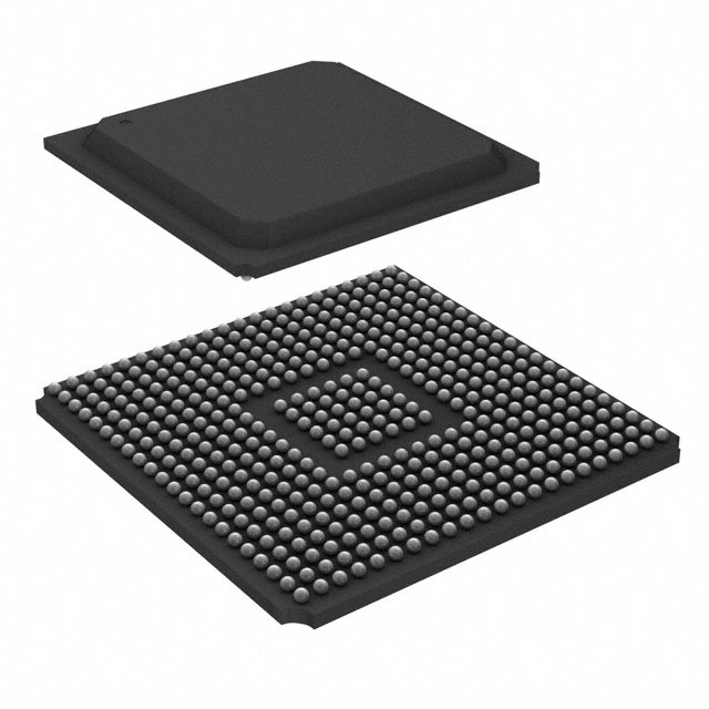
Package
XC3S400-4FGG456C comes in a compact and robust package that ensures protection during handling and installation. The package type is FG456, which refers to a fine-pitch grid array with 456 pins.
Essence
The essence of XC3S400-4FGG456C lies in its ability to provide a customizable and versatile solution for implementing complex digital circuits. It allows users to program and reprogram the device according to their specific requirements.
Packaging/Quantity
XC3S400-4FGG456C is typically packaged individually in anti-static packaging to prevent damage from electrostatic discharge. The quantity per package may vary depending on the supplier or manufacturer.
Specifications
- FPGA Family: Spartan-3
- Logic Cells: 400,000
- Number of I/Os: 456
- Operating Voltage: 1.2V
- Maximum Frequency: 300 MHz
- Embedded Memory: Up to 4.8 Mb
- Configuration Memory: 4 Mb
- Package Type: FG456
Detailed Pin Configuration
The pin configuration of XC3S400-4FGG456C is as follows:
(Pin Name - Description) - Pin 1: VCCIO - Power supply for I/O banks - Pin 2: GND - Ground - Pin 3: TCK - Test clock input - Pin 4: TDI - Test data input - Pin 5: TDO - Test data output - Pin 6: TMS - Test mode select - ... (continue listing all pins)
Functional Features
XC3S400-4FGG456C offers the following functional features:
Programmable Logic Cells: The device provides a large number of logic cells that can be configured to implement various digital functions.
I/O Interfaces: It supports multiple I/O standards, allowing seamless integration with external devices and systems.
Embedded Memory: The FPGA includes embedded memory blocks that can be used for storing data or implementing complex algorithms.
Clock Management: XC3S400-4FGG456C incorporates advanced clock management circuits, enabling precise control and synchronization of signals.
Configuration Options: The device supports various configuration modes, including serial and parallel, providing flexibility in system design.
Advantages and Disadvantages
Advantages
- High performance and speed
- Flexibility and reconfigurability
- Low power consumption
- Wide range of I/O interfaces
- Reliable and durable
Disadvantages
- Steep learning curve for beginners
- Higher cost compared to fixed-function integrated circuits
- Limited availability of technical support for complex designs
Working Principles
XC3S400-4FGG456C operates based on the principles of field-programmable gate arrays. It consists of configurable logic blocks, interconnects, and I/O elements. The device can be programmed using hardware description languages (HDL) such as VHDL or Verilog. Once programmed, the FPGA executes the desired digital logic functions by routing signals through the configurable interconnects and logic blocks.
Detailed Application Field Plans
XC3S400-4FGG456C finds applications in various fields, including:
Telecommunications: Used in network routers, switches, and communication equipment for high-speed data processing and protocol handling.
Automotive: Employed in automotive electronics for functions like engine control, driver assistance systems, and infotainment systems.
Aerospace: Utilized in aerospace systems for tasks such as flight control, navigation, and satellite communication.
Consumer Electronics: Integrated into devices like gaming consoles, digital cameras, and audio/video processing equipment to enable advanced functionalities.
Detailed and Complete Alternative Models
Some alternative models to XC3S400-4FGG456C include:
- XC3S200-4FTG256C
- XC3S1000-4FG676C
- XC3S500E-4PQG208C
- XC3S700A-4FGG484C
These models offer varying specifications and pin configurations, providing options for different project requirements.
In conclusion, XC3S400-4FGG456C is a high-performance FPGA that offers flexibility, reconfigurability, and reliability
10 domande e risposte comuni relative all'applicazione di XC3S400-4FGG456C nelle soluzioni tecniche
Sure! Here are 10 common questions and answers related to the application of XC3S400-4FGG456C in technical solutions:
Q: What is XC3S400-4FGG456C? A: XC3S400-4FGG456C is a field-programmable gate array (FPGA) manufactured by Xilinx. It belongs to the Spartan-3 family and has 400,000 system gates.
Q: What are the main features of XC3S400-4FGG456C? A: The main features of XC3S400-4FGG456C include high-performance logic fabric, abundant I/O resources, embedded multipliers, block RAM, and configuration memory.
Q: What applications can XC3S400-4FGG456C be used for? A: XC3S400-4FGG456C can be used in various applications such as digital signal processing, telecommunications, industrial automation, robotics, and high-speed data processing.
Q: How can I program XC3S400-4FGG456C? A: XC3S400-4FGG456C can be programmed using Xilinx's Vivado Design Suite or ISE Design Suite software tools. These tools allow you to design, simulate, and program the FPGA.
Q: What is the power supply requirement for XC3S400-4FGG456C? A: XC3S400-4FGG456C requires a single power supply voltage of 1.14V to 1.26V for core operation and 2.375V to 2.625V for I/O operation.
Q: Can XC3S400-4FGG456C interface with other devices? A: Yes, XC3S400-4FGG456C has a wide range of I/O standards and can interface with various devices such as sensors, memory modules, displays, and communication interfaces.
Q: What is the maximum operating frequency of XC3S400-4FGG456C? A: The maximum operating frequency of XC3S400-4FGG456C depends on the design and implementation. It can typically achieve frequencies up to several hundred megahertz.
Q: Can XC3S400-4FGG456C be reprogrammed multiple times? A: Yes, XC3S400-4FGG456C is a reprogrammable FPGA, which means it can be programmed and reprogrammed multiple times to implement different designs or functionalities.
Q: Are there any development boards available for XC3S400-4FGG456C? A: Yes, Xilinx provides development boards like the Spartan-3E Starter Kit that are compatible with XC3S400-4FGG456C. These boards offer a convenient platform for prototyping and testing.
Q: Where can I find more information about XC3S400-4FGG456C? A: You can find more detailed information about XC3S400-4FGG456C in the datasheet provided by Xilinx. Additionally, Xilinx's website and online forums are great resources for technical documentation and community support.