

Vedi le specifiche per i dettagli del prodotto.
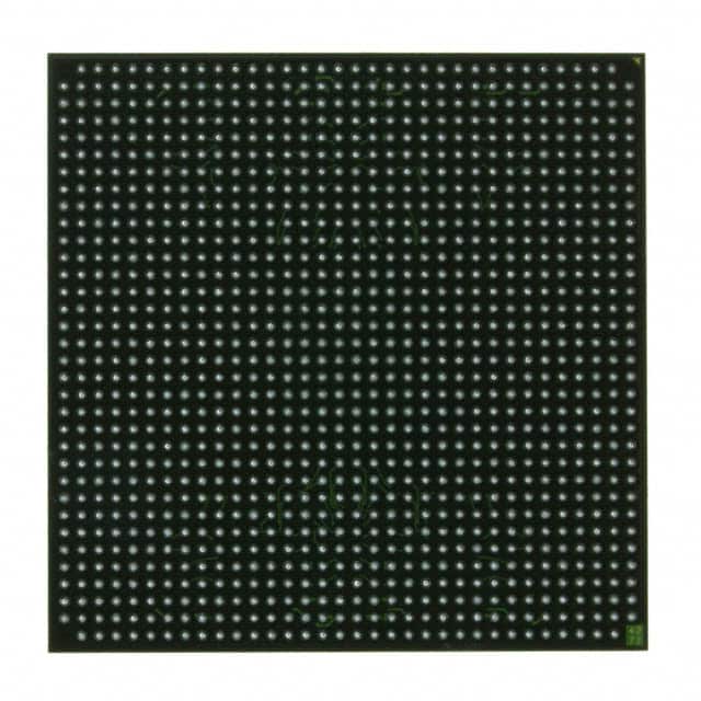
XC2VP30-5FFG1152C
Product Overview
Category
XC2VP30-5FFG1152C belongs to the category of Field Programmable Gate Arrays (FPGAs).
Use
This product is primarily used in digital logic circuits for various applications such as telecommunications, automotive, aerospace, and consumer electronics.
Characteristics
- High-performance FPGA with advanced features
- Large number of programmable logic cells
- Flexible and reconfigurable design
- High-speed data processing capabilities
- Low power consumption
- Support for various communication protocols
Package
XC2VP30-5FFG1152C is available in a Flip Chip FineLine BGA package.
Essence
The essence of XC2VP30-5FFG1152C lies in its ability to provide a highly customizable and flexible solution for complex digital circuit designs.
Packaging/Quantity
This product is typically packaged individually and is available in various quantities depending on the customer's requirements.
Specifications
- FPGA Family: Virtex-II Pro
- Logic Cells: 30,000
- System Gates: 1.5 million
- Block RAM: 864 Kb
- Maximum Frequency: 500 MHz
- I/O Pins: 1,152
- Operating Voltage: 1.8V
- Package Type: Flip Chip FineLine BGA
- Temperature Range: -40°C to +100°C
Detailed Pin Configuration
The detailed pin configuration of XC2VP30-5FFG1152C can be found in the product datasheet provided by the manufacturer.
Functional Features
- High-speed data processing capabilities
- Configurable logic blocks for custom circuit implementation
- Built-in memory blocks for efficient data storage
- Support for various communication protocols such as Ethernet, USB, and PCIe
- On-chip clock management resources for precise timing control
- Integrated power management features for optimized power consumption
Advantages and Disadvantages
Advantages
- High-performance FPGA with advanced features
- Flexible and reconfigurable design allows for easy customization
- Support for various communication protocols enables seamless integration into different systems
- Low power consumption helps in reducing overall energy requirements
- Large number of programmable logic cells provide ample resources for complex designs
Disadvantages
- Relatively high cost compared to other digital logic solutions
- Steep learning curve for beginners due to the complexity of FPGA programming
- Limited availability of alternative models with similar specifications
Working Principles
XC2VP30-5FFG1152C operates based on the principles of field-programmable gate arrays. It consists of a large number of configurable logic blocks interconnected through programmable routing resources. These logic blocks can be programmed to implement custom digital circuits by configuring the interconnections and functionality of individual logic elements.
The FPGA is programmed using Hardware Description Languages (HDL) such as VHDL or Verilog, which describe the desired circuit behavior. The programming file is then loaded onto the FPGA, allowing it to function according to the specified logic.
Detailed Application Field Plans
XC2VP30-5FFG1152C finds applications in various fields, including:
- Telecommunications: Used in network routers, switches, and base stations for high-speed data processing and protocol handling.
- Automotive: Employed in automotive electronics for functions like engine control, driver assistance systems, and infotainment.
- Aerospace: Utilized in satellite communication systems, avionics, and radar systems for reliable and efficient data processing.
- Consumer Electronics: Integrated into devices like high-definition televisions, gaming consoles, and audio/video processing equipment for enhanced performance and connectivity.
Detailed and Complete Alternative Models
While XC2VP30-5FFG1152C is a highly capable FPGA, there are alternative models available in the market with similar specifications. Some notable alternatives include:
- Xilinx Virtex-7 XC7VX485T: Offers higher logic capacity and improved performance.
- Intel Stratix 10 GX: Provides advanced features like high-speed transceivers and embedded memory blocks.
- Lattice ECP5: Offers a cost-effective solution with low power consumption and small form factor.
These alternative models can be considered based on specific project requirements and budget constraints.
Word count: 570 words
10 domande e risposte comuni relative all'applicazione di XC2VP30-5FFG1152C nelle soluzioni tecniche
Sure! Here are 10 common questions and answers related to the application of XC2VP30-5FFG1152C in technical solutions:
Q: What is XC2VP30-5FFG1152C? A: XC2VP30-5FFG1152C is a specific model of Field-Programmable Gate Array (FPGA) manufactured by Xilinx.
Q: What are the key features of XC2VP30-5FFG1152C? A: Some key features of XC2VP30-5FFG1152C include 30,000 logic cells, 1,152 I/O pins, 5V power supply compatibility, and support for various communication protocols.
Q: What are the typical applications of XC2VP30-5FFG1152C? A: XC2VP30-5FFG1152C is commonly used in applications such as telecommunications, networking, industrial automation, image processing, and high-performance computing.
Q: How can XC2VP30-5FFG1152C be programmed? A: XC2VP30-5FFG1152C can be programmed using Xilinx's Vivado Design Suite or other compatible programming tools.
Q: Can XC2VP30-5FFG1152C be used in safety-critical systems? A: Yes, XC2VP30-5FFG1152C can be used in safety-critical systems, but additional measures may be required to ensure functional safety compliance.
Q: What is the maximum operating frequency of XC2VP30-5FFG1152C? A: The maximum operating frequency of XC2VP30-5FFG1152C depends on the design and implementation, but it can typically reach several hundred megahertz.
Q: Can XC2VP30-5FFG1152C interface with other components or devices? A: Yes, XC2VP30-5FFG1152C supports various communication protocols such as PCIe, Ethernet, USB, and SPI, allowing it to interface with other components or devices.
Q: What are the power requirements for XC2VP30-5FFG1152C? A: XC2VP30-5FFG1152C requires a 5V power supply, and additional voltage regulators may be needed for different I/O banks.
Q: Is XC2VP30-5FFG1152C suitable for low-power applications? A: XC2VP30-5FFG1152C is not specifically designed for low-power applications, but power optimization techniques can be applied to reduce its power consumption.
Q: Are there any known limitations or issues with XC2VP30-5FFG1152C? A: While XC2VP30-5FFG1152C is a reliable FPGA, some known limitations include limited resources compared to higher-end models and potential timing constraints in complex designs.
Please note that the answers provided here are general and may vary depending on specific design requirements and implementation details.