

Vedi le specifiche per i dettagli del prodotto.
XC2V4000-5FFG1517C
Product Overview
Category
XC2V4000-5FFG1517C belongs to the category of Field Programmable Gate Arrays (FPGAs).
Use
This FPGA is primarily used in digital logic circuits for various applications such as telecommunications, automotive, aerospace, and consumer electronics.
Characteristics
- High-performance programmable logic device
- Offers flexibility and reconfigurability
- Provides high-speed data processing capabilities
- Supports complex algorithms and computations
- Enables rapid prototyping and development
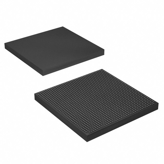
Package
XC2V4000-5FFG1517C comes in a compact and durable package that ensures protection during handling and installation.
Essence
The essence of XC2V4000-5FFG1517C lies in its ability to provide a customizable hardware platform for implementing complex digital systems.
Packaging/Quantity
This FPGA is typically packaged individually and is available in varying quantities depending on the customer's requirements.
Specifications
- Device Type: Field Programmable Gate Array (FPGA)
- Model Number: XC2V4000-5FFG1517C
- Logic Cells: 400,000
- Maximum Frequency: 500 MHz
- Operating Voltage: 1.2V
- I/O Pins: 1,517
- Package Type: Flip-Chip Fine-Pitch BGA (Ball Grid Array)
- Package Dimensions: 35mm x 35mm
Detailed Pin Configuration
The XC2V4000-5FFG1517C FPGA has a total of 1,517 pins, each serving a specific purpose in the circuit design. The detailed pin configuration can be found in the manufacturer's datasheet.
Functional Features
- High-speed data processing capabilities
- Configurable logic blocks for implementing custom logic functions
- Dedicated memory blocks for efficient data storage
- Built-in arithmetic and logic units for mathematical computations
- Programmable interconnects for flexible routing of signals
Advantages and Disadvantages
Advantages
- Flexibility and reconfigurability allow for rapid prototyping and development.
- High-performance capabilities enable the implementation of complex algorithms.
- Customizable hardware platform provides tailored solutions for various applications.
Disadvantages
- Higher power consumption compared to fixed-function integrated circuits.
- Steeper learning curve for programming and utilizing the FPGA's full potential.
- Relatively higher cost compared to traditional ASIC (Application-Specific Integrated Circuit) solutions.
Working Principles
XC2V4000-5FFG1517C operates based on the principles of digital logic design. It consists of configurable logic blocks, memory elements, and programmable interconnects. The user programs the FPGA using a Hardware Description Language (HDL) to define the desired functionality. Upon configuration, the FPGA executes the programmed logic, enabling the desired operations.
Detailed Application Field Plans
XC2V4000-5FFG1517C finds applications in various fields, including:
- Telecommunications: Used in network routers, switches, and base stations for high-speed data processing and protocol handling.
- Automotive: Employed in advanced driver-assistance systems (ADAS), engine control units (ECUs), and infotainment systems for enhanced performance and functionality.
- Aerospace: Utilized in avionics systems, satellite communication, and radar systems for reliable and efficient data processing.
- Consumer Electronics: Integrated into smart TVs, gaming consoles, and wearable devices to enable advanced features and improved performance.
Detailed and Complete Alternative Models
- XC2V6000-6FFG1152C: Similar to XC2V4000-5FFG1517C but with higher logic capacity and more I/O pins.
- XC7A100T-1FGG484C: A newer FPGA model with enhanced performance and lower power consumption.
- EP4CE115F29C7N: An alternative FPGA from a different manufacturer, offering similar capabilities.
These alternative models provide users with options based on their specific requirements and project constraints.
Word count: 550 words
10 domande e risposte comuni relative all'applicazione di XC2V4000-5FFG1517C nelle soluzioni tecniche
Sure! Here are 10 common questions and answers related to the application of XC2V4000-5FFG1517C in technical solutions:
Q: What is XC2V4000-5FFG1517C? A: XC2V4000-5FFG1517C is a specific model of Field Programmable Gate Array (FPGA) manufactured by Xilinx.
Q: What are the key features of XC2V4000-5FFG1517C? A: Some key features include 4,000 logic cells, 1,517 flip-flops, 5ns maximum delay, and support for various I/O standards.
Q: What are the typical applications of XC2V4000-5FFG1517C? A: XC2V4000-5FFG1517C is commonly used in applications such as digital signal processing, high-speed data communication, image and video processing, and control systems.
Q: How can XC2V4000-5FFG1517C be programmed? A: XC2V4000-5FFG1517C can be programmed using Hardware Description Languages (HDLs) like VHDL or Verilog, or through Xilinx's proprietary software tools.
Q: Can XC2V4000-5FFG1517C be reprogrammed after deployment? A: Yes, XC2V4000-5FFG1517C is a reprogrammable FPGA, allowing for updates and modifications to the design even after deployment.
Q: What is the power consumption of XC2V4000-5FFG1517C? A: The power consumption of XC2V4000-5FFG1517C depends on the specific design and operating conditions, but it typically ranges from a few watts to tens of watts.
Q: What are the voltage requirements for XC2V4000-5FFG1517C? A: XC2V4000-5FFG1517C operates at a core voltage of 1.5V and supports various I/O voltage standards such as 3.3V, 2.5V, and 1.8V.
Q: Can XC2V4000-5FFG1517C interface with other components or devices? A: Yes, XC2V4000-5FFG1517C can interface with other components or devices through its configurable I/O pins, supporting various protocols like UART, SPI, I2C, and more.
Q: Are there any limitations or constraints when using XC2V4000-5FFG1517C? A: Some limitations include limited resources (logic cells, flip-flops), limited memory, and potential performance bottlenecks depending on the complexity of the design.
Q: Where can I find additional documentation and support for XC2V4000-5FFG1517C? A: Xilinx provides comprehensive documentation, datasheets, application notes, and technical support for XC2V4000-5FFG1517C on their official website.