

Vedi le specifiche per i dettagli del prodotto.
XC2V3000-5BG728I
Product Overview
Category
The XC2V3000-5BG728I belongs to the category of Field Programmable Gate Arrays (FPGAs).
Use
FPGAs are integrated circuits that can be programmed and reprogrammed to perform various digital functions. The XC2V3000-5BG728I is specifically designed for high-performance applications requiring complex logic functions.
Characteristics
- High-performance FPGA with advanced features
- Large capacity and high-speed processing capabilities
- Flexible and reconfigurable design
- Suitable for demanding applications in industries such as telecommunications, aerospace, and defense
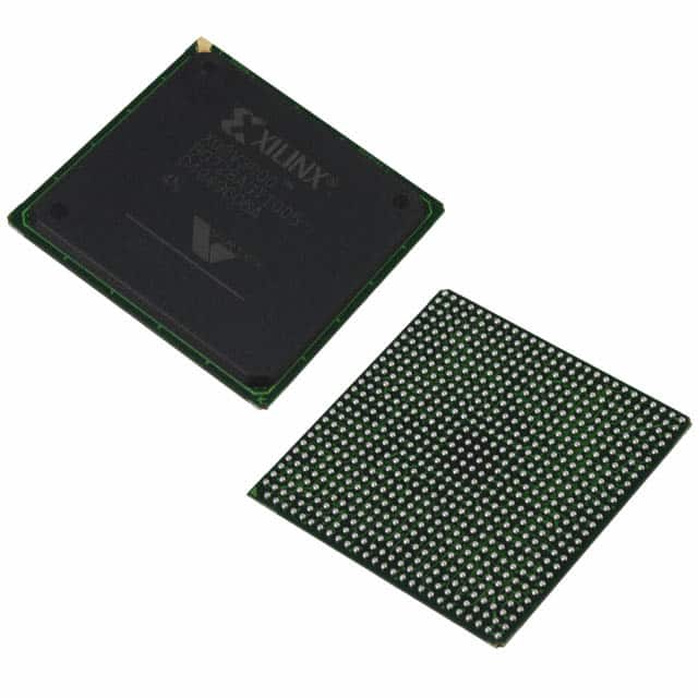
Package
The XC2V3000-5BG728I comes in a Ball Grid Array (BGA) package.
Essence
The essence of the XC2V3000-5BG728I lies in its ability to provide a customizable hardware solution for complex digital systems. It allows designers to implement their own logic functions and optimize performance according to specific requirements.
Packaging/Quantity
The XC2V3000-5BG728I is typically packaged individually and is available in varying quantities depending on customer needs.
Specifications
- FPGA Family: Virtex-II
- Logic Cells: 3,000
- System Gates: 50,000
- Maximum Frequency: 200 MHz
- I/O Pins: 728
- Operating Voltage: 1.8V
- Operating Temperature Range: -40°C to +85°C
Detailed Pin Configuration
The XC2V3000-5BG728I has 728 I/O pins, each serving a specific purpose in the system. These pins are organized into different banks and groups, providing flexibility in connecting external devices and peripherals.
For a detailed pin configuration diagram, please refer to the datasheet provided by the manufacturer.
Functional Features
- High-speed processing: The XC2V3000-5BG728I offers fast data processing capabilities, making it suitable for applications requiring real-time performance.
- Reconfigurability: The FPGA can be reprogrammed to adapt to changing requirements or to fix errors without the need for hardware changes.
- Embedded memory: The device includes embedded memory blocks that can be used for storing data or implementing complex algorithms.
- Flexible I/O options: The XC2V3000-5BG728I supports a wide range of I/O standards, allowing seamless integration with various external devices.
Advantages and Disadvantages
Advantages
- Customizability: FPGAs provide the ability to implement custom logic functions, offering flexibility in system design.
- High-performance: The XC2V3000-5BG728I delivers high-speed processing capabilities, enabling efficient execution of complex tasks.
- Reusability: The FPGA can be reprogrammed multiple times, making it suitable for prototyping and iterative development processes.
Disadvantages
- Complexity: Designing and programming FPGAs require specialized knowledge and expertise.
- Power consumption: FPGAs tend to consume more power compared to other integrated circuits, which may be a concern in certain applications.
- Cost: FPGAs can be relatively expensive compared to other off-the-shelf integrated circuits, especially for low-volume production.
Working Principles
The XC2V3000-5BG728I operates based on the principles of configurable logic. It consists of an array of programmable logic cells interconnected through configurable routing resources. These logic cells can be programmed to perform specific functions, such as arithmetic operations, data storage, or control logic. The configuration is stored in internal memory elements, allowing the FPGA to retain its functionality even after power cycles.
Detailed Application Field Plans
The XC2V3000-5BG728I finds applications in various industries, including:
- Telecommunications: Used in high-speed data processing systems, network routers, and communication infrastructure.
- Aerospace: Employed in avionics systems, satellite communication, and radar signal processing.
- Defense: Utilized in military-grade equipment, secure communication systems, and electronic warfare applications.
- Industrial Automation: Applied in control systems, robotics, and machine vision applications.
- Medical Devices: Integrated into medical imaging systems, patient monitoring devices, and diagnostic equipment.
Detailed and Complete Alternative Models
- XC2V2000-4FG676I: A lower-capacity variant of the same FPGA family, suitable for applications with less demanding requirements.
- XC2V4000-6FF1152C: A higher-capacity variant with increased logic cells and system gates, offering enhanced performance for complex designs.
- XC2S50-5TQ144C: An alternative FPGA from a different family, providing a cost-effective solution for smaller-scale applications.
These alternative models offer different capacity, performance, and cost trade-offs, allowing designers to choose the most suitable FPGA for their specific application requirements.
*Word count:
10 domande e risposte comuni relative all'applicazione di XC2V3000-5BG728I nelle soluzioni tecniche
Sure! Here are 10 common questions and answers related to the application of XC2V3000-5BG728I in technical solutions:
Q: What is XC2V3000-5BG728I? A: XC2V3000-5BG728I is a specific model of Field-Programmable Gate Array (FPGA) manufactured by Xilinx.
Q: What are the key features of XC2V3000-5BG728I? A: Some key features of XC2V3000-5BG728I include 3,000 logic cells, 5ns maximum delay, and 728-ball grid array packaging.
Q: In what technical solutions can XC2V3000-5BG728I be used? A: XC2V3000-5BG728I can be used in various applications such as digital signal processing, telecommunications, aerospace, and industrial automation.
Q: How does XC2V3000-5BG728I differ from other FPGA models? A: XC2V3000-5BG728I differs from other FPGA models in terms of its specific configuration, performance characteristics, and pinout arrangement.
Q: Can XC2V3000-5BG728I be reprogrammed after deployment? A: Yes, XC2V3000-5BG728I is a field-programmable device, meaning it can be reprogrammed even after being deployed in a system.
Q: What development tools are available for programming XC2V3000-5BG728I? A: Xilinx provides software tools like Vivado Design Suite that can be used for designing, simulating, and programming XC2V3000-5BG728I.
Q: What are the power requirements for XC2V3000-5BG728I? A: XC2V3000-5BG728I typically requires a supply voltage of 1.8V or 2.5V, depending on the specific configuration.
Q: Can XC2V3000-5BG728I interface with other components or devices? A: Yes, XC2V3000-5BG728I can interface with various components and devices through its I/O pins, supporting protocols like UART, SPI, I2C, and more.
Q: Are there any limitations or considerations when using XC2V3000-5BG728I? A: Some considerations include power consumption, heat dissipation, timing constraints, and the need for proper signal integrity measures.
Q: Where can I find additional resources or support for XC2V3000-5BG728I? A: Xilinx provides documentation, application notes, forums, and technical support to assist users in working with XC2V3000-5BG728I.