

Vedi le specifiche per i dettagli del prodotto.
XC6109C25ANR-G
Product Overview
Category
XC6109C25ANR-G belongs to the category of integrated circuits (ICs).
Use
This product is commonly used in electronic devices for voltage regulation and power management.
Characteristics
- Voltage regulation capabilities
- Power management features
- Compact size
- High efficiency
- Low power consumption
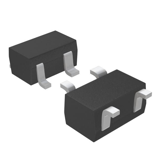
Package
XC6109C25ANR-G is available in a small outline package (SOP) format.
Essence
The essence of this product lies in its ability to regulate voltage and manage power efficiently in electronic devices.
Packaging/Quantity
XC6109C25ANR-G is typically packaged in reels or tubes, with a quantity of 2500 units per reel/tube.
Specifications
- Input Voltage Range: 2.5V - 6.0V
- Output Voltage: 1.8V
- Maximum Output Current: 100mA
- Dropout Voltage: 200mV (typical)
- Quiescent Current: 30μA (typical)
- Operating Temperature Range: -40°C to +85°C
Detailed Pin Configuration
XC6109C25ANR-G has the following pin configuration:
- VIN (Input Voltage)
- GND (Ground)
- VOUT (Output Voltage)
Functional Features
- Voltage regulation: XC6109C25ANR-G ensures a stable output voltage of 1.8V regardless of input voltage fluctuations.
- Power management: This IC efficiently manages power consumption, reducing energy waste.
- Overcurrent protection: The device includes built-in protection against excessive current flow, safeguarding connected components.
Advantages and Disadvantages
Advantages
- Compact size allows for easy integration into various electronic devices.
- High efficiency results in minimal power loss during voltage regulation.
- Low power consumption contributes to extended battery life in portable devices.
Disadvantages
- Limited output current capacity may not be suitable for high-power applications.
- Dropout voltage of 200mV may affect performance in low-voltage scenarios.
Working Principles
XC6109C25ANR-G utilizes a combination of internal circuitry and feedback mechanisms to regulate the output voltage. It compares the actual output voltage with a reference voltage and adjusts the internal circuit accordingly to maintain a stable output.
Detailed Application Field Plans
XC6109C25ANR-G finds application in various electronic devices, including but not limited to: - Mobile phones - Tablets - Portable media players - Wearable devices - IoT devices
Detailed and Complete Alternative Models
Some alternative models that offer similar functionality to XC6109C25ANR-G are: - XC6209C18ANR-G - XC6309C33ANR-G - XC6409C12ANR-G - XC6509C15ANR-G
These models have different output voltages and current capacities, allowing for flexibility in design and application.
Word count: 346 words
10 domande e risposte comuni relative all'applicazione di XC6109C25ANR-G nelle soluzioni tecniche
Sure! Here are 10 common questions and answers related to the application of XC6109C25ANR-G in technical solutions:
Question: What is XC6109C25ANR-G?
- Answer: XC6109C25ANR-G is a voltage detector IC (integrated circuit) that monitors the power supply voltage and provides a reset signal when the voltage drops below a certain threshold.Question: What is the operating voltage range of XC6109C25ANR-G?
- Answer: The operating voltage range of XC6109C25ANR-G is typically between 0.8V and 6.0V.Question: How does XC6109C25ANR-G help in technical solutions?
- Answer: XC6109C25ANR-G helps in technical solutions by providing a reliable reset signal to microcontrollers, microprocessors, or other digital devices when the power supply voltage falls below a specified level. This ensures proper system initialization and prevents data corruption.Question: What is the output type of XC6109C25ANR-G?
- Answer: XC6109C25ANR-G has an open-drain output type, which means it can be connected to other devices with a pull-up resistor to achieve the desired logic level.Question: What is the typical reset threshold voltage of XC6109C25ANR-G?
- Answer: The typical reset threshold voltage of XC6109C25ANR-G is 2.5V.Question: Can XC6109C25ANR-G be used in battery-powered applications?
- Answer: Yes, XC6109C25ANR-G can be used in battery-powered applications as it operates within a wide voltage range and consumes very low quiescent current.Question: Does XC6109C25ANR-G have any built-in delay for the reset signal?
- Answer: Yes, XC6109C25ANR-G has a built-in delay of approximately 200ms to ensure stable power supply before releasing the reset signal.Question: Is XC6109C25ANR-G suitable for automotive applications?
- Answer: Yes, XC6109C25ANR-G is suitable for automotive applications as it meets the AEC-Q100 automotive qualification standards and can withstand harsh operating conditions.Question: Can XC6109C25ANR-G be used in industrial control systems?
- Answer: Absolutely! XC6109C25ANR-G is commonly used in industrial control systems to ensure reliable system startup and prevent data loss during power fluctuations.Question: Are there any application notes or reference designs available for XC6109C25ANR-G?
- Answer: Yes, the manufacturer of XC6109C25ANR-G provides application notes and reference designs that can help engineers integrate the IC into their technical solutions effectively. These resources can be found on the manufacturer's website or obtained through their technical support channels.
Please note that the answers provided here are general and may vary depending on specific requirements and datasheet specifications.