

Vedi le specifiche per i dettagli del prodotto.
TPS65573DSST
Product Overview
Category
The TPS65573DSST belongs to the category of integrated circuits (ICs) specifically designed for power management applications.
Use
This IC is commonly used in various electronic devices and systems to efficiently regulate power supply, voltage conversion, and control functions.
Characteristics
- High efficiency: The TPS65573DSST offers high conversion efficiency, minimizing power losses during operation.
- Wide input voltage range: It can handle a wide range of input voltages, making it suitable for diverse applications.
- Compact package: The IC is available in a small form factor package, enabling space-saving designs.
- Low power consumption: It consumes minimal power during standby or idle modes, enhancing overall energy efficiency.
Package and Quantity
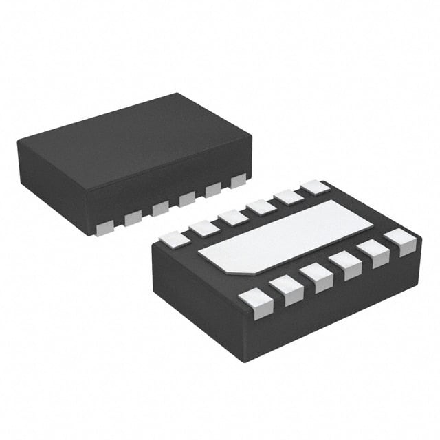
The TPS65573DSST is typically packaged in a compact surface-mount package, such as a QFN (Quad Flat No-leads) package. The exact package dimensions and pin configuration are detailed below. It is commonly supplied in reels or trays containing multiple units, depending on the manufacturer's specifications.
Specifications
- Input Voltage Range: 2.7V to 5.5V
- Output Voltage Range: Adjustable, typically up to 5V
- Maximum Output Current: 500mA
- Operating Temperature Range: -40°C to +85°C
- Switching Frequency: Adjustable, typically up to 2MHz
- Control Interface: I2C (Inter-Integrated Circuit)
Pin Configuration
The TPS65573DSST features a specific pin configuration that facilitates its integration into various circuit designs. The following diagram illustrates the pinout and their corresponding functions:

- VIN: Input voltage supply
- GND: Ground reference
- EN: Enable pin for controlling the IC's operation
- VOUT: Output voltage
- FB: Feedback pin for voltage regulation
- SDA: Serial Data Line (I2C interface)
- SCL: Serial Clock Line (I2C interface)
Functional Features
The TPS65573DSST offers several functional features that enhance its performance and versatility:
- Voltage Regulation: The IC provides precise voltage regulation, ensuring stable output voltages even under varying load conditions.
- Power Sequencing: It supports power sequencing capabilities, enabling controlled power-up and power-down sequences in complex systems.
- Fault Protection: The IC incorporates various protection mechanisms, such as overvoltage protection, undervoltage lockout, and thermal shutdown, safeguarding the device and the connected circuitry from potential damage.
Advantages and Disadvantages
Advantages
- High efficiency leads to reduced power consumption and extended battery life in portable devices.
- Wide input voltage range allows compatibility with different power sources.
- Compact package enables space-efficient designs.
- Integrated fault protection enhances system reliability.
Disadvantages
- Limited maximum output current may restrict usage in high-power applications.
- Control interface limited to I2C protocol, which may not be compatible with all systems.
Working Principles
The TPS65573DSST operates based on a switching regulator topology, utilizing pulse-width modulation (PWM) techniques to regulate the output voltage. It employs an internal control loop that continuously monitors the output voltage and adjusts the duty cycle of the switching transistor accordingly. This feedback mechanism ensures a stable and accurate output voltage despite variations in input voltage or load conditions.
Detailed Application Field Plans
The TPS65573DSST finds application in various electronic devices and systems, including but not limited to: - Portable consumer electronics (e.g., smartphones, tablets, portable media players) - Wearable devices (e.g., smartwatches, fitness trackers) - Internet of Things (IoT) devices - Industrial automation systems - Automotive electronics
Alternative Models
For users seeking alternative options, the following ICs can be considered as substitutes for the TPS65573DSST: - TPS65574DSST - TPS65575DSST - TPS65576DSST
These alternatives offer similar functionality and characteristics, providing flexibility in design choices.
In conclusion, the TPS65573DSST is a highly efficient integrated circuit designed for power management applications. Its compact package, wide input voltage range, and various functional features make it suitable for diverse electronic devices and systems. While it has certain limitations, its advantages outweigh the disadvantages, making it a popular choice among designers.
10 domande e risposte comuni relative all'applicazione di TPS65573DSST nelle soluzioni tecniche
Sure! Here are 10 common questions and answers related to the application of TPS65573DSST in technical solutions:
Q: What is TPS65573DSST? A: TPS65573DSST is a power management integrated circuit (PMIC) designed for use in various technical solutions.
Q: What are the key features of TPS65573DSST? A: Some key features of TPS65573DSST include multiple voltage regulators, power sequencing, fault protection, and low quiescent current.
Q: What technical solutions can TPS65573DSST be used in? A: TPS65573DSST can be used in a wide range of applications such as industrial automation, automotive systems, consumer electronics, and more.
Q: How many voltage regulators does TPS65573DSST have? A: TPS65573DSST has three integrated voltage regulators, which can provide different output voltages as per the requirements.
Q: Can TPS65573DSST handle power sequencing? A: Yes, TPS65573DSST has built-in power sequencing capabilities, allowing for proper startup and shutdown sequences of different power rails.
Q: Does TPS65573DSST offer any fault protection features? A: Yes, TPS65573DSST provides various fault protection mechanisms like overvoltage protection, undervoltage lockout, and thermal shutdown.
Q: What is the quiescent current of TPS65573DSST? A: TPS65573DSST has a low quiescent current, typically in the microampere range, which helps in reducing power consumption during standby or idle modes.
Q: Can TPS65573DSST operate in harsh environments? A: Yes, TPS65573DSST is designed to operate reliably in harsh environments with a wide temperature range and robust protection features.
Q: Is TPS65573DSST compatible with other power management ICs? A: Yes, TPS65573DSST can be easily integrated with other power management ICs to create more complex power solutions if needed.
Q: Where can I find more information about the application of TPS65573DSST? A: You can refer to the datasheet, application notes, or contact the manufacturer for more detailed information on the application of TPS65573DSST in technical solutions.
Please note that the answers provided here are general and may vary depending on specific use cases and requirements.