

Vedi le specifiche per i dettagli del prodotto.
TAS5612LADDV
Product Overview
The TAS5612LADDV belongs to the category of audio amplifier integrated circuits. It is commonly used in audio systems for amplifying and processing audio signals. The characteristics of this product include high efficiency, low distortion, and a compact package. The essence of TAS5612LADDV lies in its ability to deliver high-quality audio amplification while minimizing power consumption. It is typically packaged in small, surface-mount packages and is available in various quantities.
Specifications
- Power Supply Range: 4.5V to 26.4V
- Output Power: Up to 150W per channel
- Total Harmonic Distortion + Noise: <0.1%
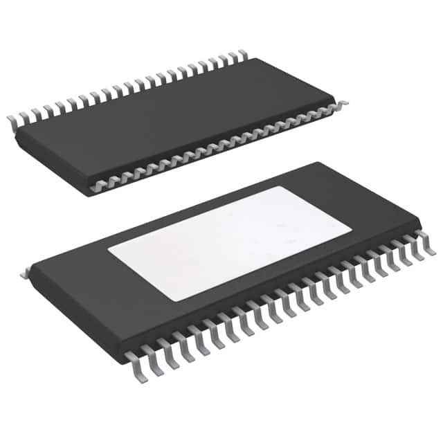
- Package Type: PowerPAD-HTQFP
Detailed Pin Configuration
The TAS5612LADDV features a comprehensive pin configuration that includes inputs for audio signals, power supply connections, and output channels. The detailed pinout can be found in the product datasheet.
Functional Features
- Advanced Audio Processing: The TAS5612LADDV integrates advanced audio processing algorithms for improved sound quality.
- Digital Input Interface: It supports various digital input interfaces such as I2S and TDM, enabling seamless integration with digital audio sources.
- Protection Circuitry: Built-in protection circuitry safeguards the amplifier and connected speakers from overloads and short circuits.
Advantages and Disadvantages
Advantages
- High Efficiency: The TAS5612LADDV offers high efficiency, making it suitable for battery-powered applications.
- Low Distortion: It delivers low distortion audio output, ensuring high fidelity sound reproduction.
- Compact Package: Its compact package makes it suitable for space-constrained designs.
Disadvantages
- Complexity: The advanced features of TAS5612LADDV may require additional expertise for optimal utilization.
- Cost: It may have a higher cost compared to basic audio amplifier ICs.
Working Principles
The TAS5612LADDV operates by receiving digital audio signals, processing them using internal algorithms, and amplifying the processed signals to drive connected speakers. Its high-efficiency design minimizes power loss, resulting in reduced heat dissipation.
Detailed Application Field Plans
The TAS5612LADDV is well-suited for a wide range of audio applications including: - Home Theater Systems - Professional Audio Equipment - Automotive Infotainment Systems - Portable Bluetooth Speakers
Detailed and Complete Alternative Models
- TAS5612LA: A lower power variant suitable for applications with lower power requirements.
- TAS5613LADDV: A similar amplifier IC with additional features for enhanced audio processing.
In conclusion, the TAS5612LADDV is a versatile audio amplifier IC with advanced features, making it suitable for various audio applications where high-quality sound reproduction is essential.
Word Count: 345
10 domande e risposte comuni relative all'applicazione di TAS5612LADDV nelle soluzioni tecniche
Sure, here are 10 common questions and answers related to the application of TAS5612LADDV in technical solutions:
Q: What is TAS5612LADDV? A: TAS5612LADDV is a high-performance digital input Class D amplifier with integrated closed-loop feedback technology.
Q: What is the typical application of TAS5612LADDV? A: TAS5612LADDV is commonly used in audio applications such as home theater systems, soundbars, and multimedia speakers.
Q: What is the maximum output power of TAS5612LADDV? A: TAS5612LADDV can deliver up to 150W per channel into a 4-Ω load or 100W per channel into an 8-Ω load.
Q: What are the key features of TAS5612LADDV? A: The key features of TAS5612LADDV include advanced protection circuitry, integrated feedback loop compensation, and support for various input formats.
Q: Can TAS5612LADDV be used in bridge-tied load (BTL) configuration? A: Yes, TAS5612LADDV supports BTL configuration for higher output power applications.
Q: What is the recommended power supply voltage for TAS5612LADDV? A: The recommended power supply voltage range for TAS5612LADDV is typically between 18V and 36V.
Q: Does TAS5612LADDV require external heat sinking? A: Yes, TAS5612LADDV may require external heat sinking depending on the application and power dissipation requirements.
Q: Is TAS5612LADDV compatible with digital signal processors (DSPs)? A: Yes, TAS5612LADDV is compatible with most digital signal processors and can be integrated into DSP-based audio systems.
Q: What kind of input interfaces does TAS5612LADDV support? A: TAS5612LADDV supports various input interfaces including I2S, TDM, and S/PDIF, making it versatile for different digital audio sources.
Q: Are evaluation modules available for TAS5612LADDV? A: Yes, evaluation modules and reference designs are available to help developers quickly prototype and evaluate TAS5612LADDV in their technical solutions.