

Vedi le specifiche per i dettagli del prodotto.
SN74LVTH16374GRDR
Product Overview
- Category: Integrated Circuit (IC)
- Use: Logic Level Shifter
- Characteristics: High-speed, low-voltage, 16-bit D-type flip-flop with 3-state outputs
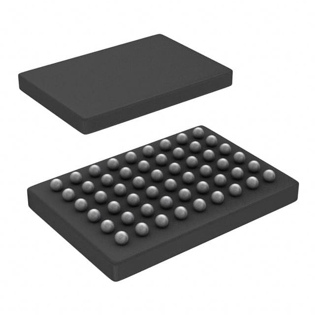
- Package: Green, plastic, 56-pin Very Thin Quad Flat Package (VQFN)
- Essence: Logic level shifting and storage of digital signals
- Packaging/Quantity: Tape and reel packaging, 2500 units per reel
Specifications
- Supply Voltage Range: 2.7V to 3.6V
- Input Voltage Range: 0V to VCC
- Output Voltage Range: 0V to VCC
- High-Level Input Voltage: 2.0V to VCC + 0.5V
- Low-Level Input Voltage: -0.5V to 0.8V
- High-Level Output Voltage: VCC - 0.4V
- Low-Level Output Voltage: 0.4V
- Maximum Operating Frequency: 200MHz
- Propagation Delay Time: 2.1ns (typical)
Detailed Pin Configuration
The SN74LVTH16374GRDR has a total of 56 pins, which are organized as follows:
- Pin 1: GND (Ground)
- Pin 2: Q0 (Output 0)
- Pin 3: Q1 (Output 1)
- ...
- Pin 54: Q14 (Output 14)
- Pin 55: Q15 (Output 15)
- Pin 56: VCC (Supply Voltage)
Functional Features
- 16-bit D-type flip-flop with 3-state outputs
- Provides voltage level shifting between different logic families
- Supports bidirectional data flow
- High-speed operation with minimal propagation delay
- Low power consumption
- 3-state outputs allow multiple devices to share a common bus
Advantages and Disadvantages
Advantages: - High-speed operation enables efficient data transfer - Low-voltage operation reduces power consumption - 3-state outputs facilitate bus sharing in multi-device systems
Disadvantages: - Limited voltage range (2.7V to 3.6V) - Not suitable for applications requiring higher operating frequencies
Working Principles
The SN74LVTH16374GRDR is designed to shift logic levels between different voltage domains. It consists of 16 D-type flip-flops with 3-state outputs. The inputs are latched on the rising edge of the clock signal, and the output states can be controlled by the output enable (OE) pin.
When the OE pin is high, the outputs are in the high-impedance state, allowing other devices to drive the shared bus. When the OE pin is low, the outputs reflect the stored data from the inputs.
The IC operates within a specified supply voltage range and provides reliable level shifting while maintaining high-speed performance.
Detailed Application Field Plans
The SN74LVTH16374GRDR is commonly used in various digital systems where logic level shifting is required. Some application fields include:
- Microcontrollers and microprocessors: Interface between different voltage domains in embedded systems.
- Communication systems: Level shifting between different logic families (e.g., TTL and CMOS) in serial communication interfaces.
- Data acquisition systems: Conversion of analog signals to digital levels using ADCs and subsequent level shifting for processing.
- Industrial automation: Interfacing between different control modules operating at different voltage levels.
- Automotive electronics: Level shifting in automotive communication protocols such as CAN or LIN buses.
Detailed and Complete Alternative Models
- SN74LVC16374ADGVR: Similar 16-bit D-type flip-flop with 3-state outputs, but operates at a lower voltage range (1.65V to 3.6V).
- SN74LVTH16373DLR: 16-bit transparent D-type latch with 3-state outputs, suitable for applications requiring level shifting and latching functionality.
- SN74LVC16374AZQLR: 16-bit D-type flip-flop with 3-state outputs in a smaller package (56-pin LLP).
These alternative models offer similar functionality with slight variations in voltage range, package type, or additional features.
In conclusion, the SN74LVTH16374GRDR is a high-speed, low-voltage logic level shifter integrated circuit. It provides reliable voltage level shifting between different logic families and finds applications in various digital systems. Its advantages include high-speed operation, low power consumption, and support for bus sharing. However, it has limitations in terms of voltage range and operating frequency. Alternative models with different specifications are available to suit specific application requirements.
10 domande e risposte comuni relative all'applicazione di SN74LVTH16374GRDR nelle soluzioni tecniche
What is the maximum operating voltage for SN74LVTH16374GRDR?
- The maximum operating voltage for SN74LVTH16374GRDR is 3.6V.What is the typical input threshold voltage for SN74LVTH16374GRDR?
- The typical input threshold voltage for SN74LVTH16374GRDR is 1.5V.What is the maximum propagation delay for SN74LVTH16374GRDR?
- The maximum propagation delay for SN74LVTH16374GRDR is 4.1ns.Can SN74LVTH16374GRDR be used in automotive applications?
- Yes, SN74LVTH16374GRDR is suitable for automotive applications.What is the package type for SN74LVTH16374GRDR?
- SN74LVTH16374GRDR comes in a TSSOP package.Is SN74LVTH16374GRDR RoHS compliant?
- Yes, SN74LVTH16374GRDR is RoHS compliant.What is the maximum operating temperature range for SN74LVTH16374GRDR?
- The maximum operating temperature range for SN74LVTH16374GRDR is -40°C to 85°C.Can SN74LVTH16374GRDR be used in high-speed data transfer applications?
- Yes, SN74LVTH16374GRDR is suitable for high-speed data transfer applications.Does SN74LVTH16374GRDR have built-in ESD protection?
- Yes, SN74LVTH16374GRDR has built-in ESD protection.What is the recommended supply voltage for SN74LVTH16374GRDR?
- The recommended supply voltage for SN74LVTH16374GRDR is 3.3V.