

Vedi le specifiche per i dettagli del prodotto.
SN74LVC1G97YZPR
Product Overview
- Category: Integrated Circuit
- Use: Logic Gate
- Characteristics: Single 2-input Multiplexer
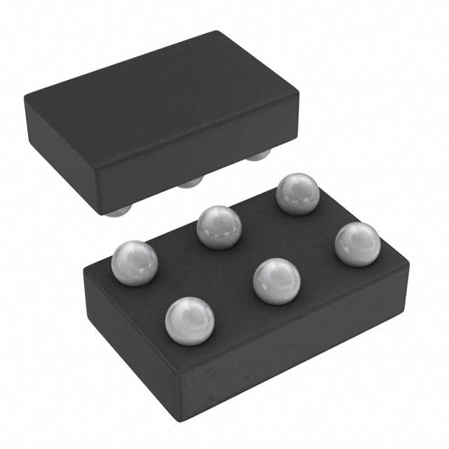
- Package: DSBGA (Y)
- Essence: High-Speed CMOS Logic
- Packaging/Quantity: Tape and Reel, 3000 pieces per reel
Specifications
- Supply Voltage Range: 1.65V to 5.5V
- Input Voltage Range: -0.5V to VCC + 0.5V
- Output Voltage Range: 0V to VCC
- Maximum Operating Frequency: 400MHz
- Propagation Delay: 3.8ns (typical)
- Low Power Consumption: ICC = 4µA (maximum)
Detailed Pin Configuration
The SN74LVC1G97YZPR has the following pin configuration:
____
   A1 |    | VCC
   B1 |    | Y1
 GND1 |    | S1
   A2 |    | S2
   B2 |    | Y2
 GND2 |____| NC
Functional Features
- Single 2-input multiplexer with output enable
- Wide supply voltage range allows compatibility with various systems
- High-speed operation suitable for applications requiring fast switching
- Low power consumption ensures energy efficiency
- Small package size enables space-saving designs
Advantages and Disadvantages
Advantages: - Wide supply voltage range provides flexibility in system integration - High-speed operation allows for efficient data processing - Low power consumption reduces energy usage and extends battery life - Small package size enables compact circuit designs
Disadvantages: - Limited to 2-input multiplexing functionality - Not suitable for applications requiring more complex logic operations
Working Principles
The SN74LVC1G97YZPR is a single 2-input multiplexer with an output enable feature. It operates using high-speed CMOS logic, allowing for fast switching between input signals. The device can be powered by a supply voltage ranging from 1.65V to 5.5V, making it compatible with various systems. When the output enable (OE) pin is low, the selected input signal is passed through to the output pin. Conversely, when OE is high, the output is disabled and remains in a high-impedance state.
Detailed Application Field Plans
The SN74LVC1G97YZPR is commonly used in applications that require signal multiplexing or data routing. Some specific application fields include:
- Communication Systems: The device can be utilized in communication systems to switch between different data sources or channels.
- Consumer Electronics: It can be integrated into consumer electronic devices such as smartphones, tablets, and digital cameras for signal routing purposes.
- Industrial Automation: The multiplexer finds applications in industrial automation systems where multiple sensors or inputs need to be selectively processed.
- Automotive Electronics: In automotive electronics, the SN74LVC1G97YZPR can be employed for signal routing and data selection in various control modules.
Detailed and Complete Alternative Models
- SN74LVC1G98YZPR: Similar to SN74LVC1G97YZPR but with inverted outputs.
- SN74LVC1G99YZPR: Dual 2-input multiplexer with output enable.
- SN74LVC2G53YZPR: Dual 2-channel analog multiplexer/demultiplexer.
These alternative models offer similar functionality and characteristics, providing options for different design requirements.
Word count: 399 words
10 domande e risposte comuni relative all'applicazione di SN74LVC1G97YZPR nelle soluzioni tecniche
Sure! Here are 10 common questions and answers related to the application of SN74LVC1G97YZPR:
Q1: What is SN74LVC1G97YZPR? A1: SN74LVC1G97YZPR is a single buffer/driver with open-drain output, designed for use in various technical solutions.
Q2: What is the voltage range supported by SN74LVC1G97YZPR? A2: SN74LVC1G97YZPR supports a voltage range from 1.65V to 5.5V.
Q3: What is the maximum output current of SN74LVC1G97YZPR? A3: The maximum output current of SN74LVC1G97YZPR is typically 32mA.
Q4: Can SN74LVC1G97YZPR be used as a level shifter? A4: Yes, SN74LVC1G97YZPR can be used as a level shifter to convert signals between different voltage levels.
Q5: What is the maximum operating frequency of SN74LVC1G97YZPR? A5: The maximum operating frequency of SN74LVC1G97YZPR is typically 100MHz.
Q6: Does SN74LVC1G97YZPR have built-in protection features? A6: Yes, SN74LVC1G97YZPR has built-in ESD protection to safeguard against electrostatic discharge.
Q7: Can SN74LVC1G97YZPR be used in battery-powered applications? A7: Yes, SN74LVC1G97YZPR can be used in battery-powered applications due to its low power consumption.
Q8: Is SN74LVC1G97YZPR compatible with other logic families? A8: Yes, SN74LVC1G97YZPR is compatible with both CMOS and TTL logic families.
Q9: Can SN74LVC1G97YZPR be used in high-speed data transmission applications? A9: Yes, SN74LVC1G97YZPR can be used in high-speed data transmission applications due to its fast switching speed.
Q10: What is the package type of SN74LVC1G97YZPR? A10: SN74LVC1G97YZPR is available in a small SOT-553 package.