

Vedi le specifiche per i dettagli del prodotto.
SN74LV175ADGVR
Product Overview
Category
SN74LV175ADGVR belongs to the category of integrated circuits (ICs).
Use
It is commonly used in electronic devices for data storage and manipulation.
Characteristics
- Low-voltage operation
- High-speed performance
- Wide operating temperature range
- Small package size
- Low power consumption
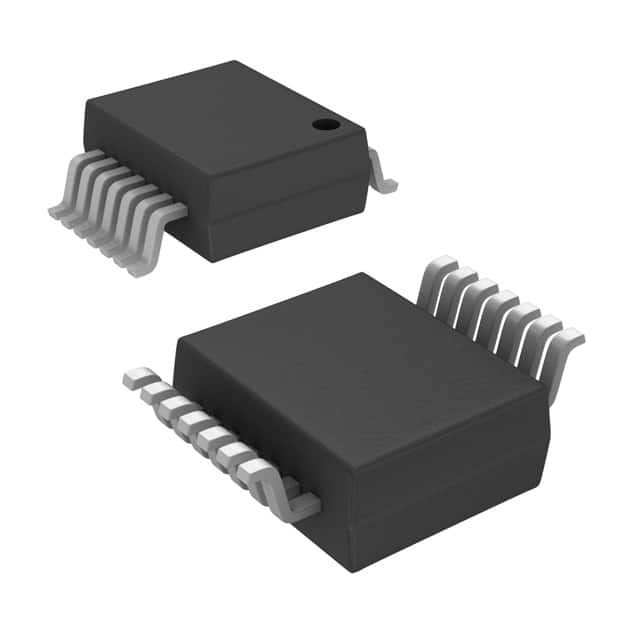
Package
SN74LV175ADGVR is available in a small form factor package, typically a VSSOP (Very Small Outline Package).
Essence
The essence of SN74LV175ADGVR lies in its ability to store and manipulate digital data efficiently.
Packaging/Quantity
SN74LV175ADGVR is usually packaged in reels or tubes, with each reel or tube containing a specific quantity of ICs. The exact quantity may vary depending on the manufacturer.
Specifications
- Supply Voltage: 2V to 5.5V
- Logic Family: LV (Low Voltage)
- Number of Flip-Flops: 4
- Input/Output Compatibility: CMOS/TTL
- Operating Temperature Range: -40°C to +85°C
- Propagation Delay: <10 ns
- Maximum Clock Frequency: 100 MHz
Detailed Pin Configuration
- CLR (Clear) - Clear input for resetting the flip-flop outputs.
- D (Data) - Data input for storing in the flip-flops.
- CP (Clock Pulse) - Clock input for synchronizing the data transfer.
- Q0-Q3 (Flip-Flop Outputs) - Outputs representing the stored data.
- GND (Ground) - Ground reference for the IC.
- Q3' (Complementary Output) - Complementary output of Q3.
- CP' (Inverted Clock Pulse) - Inverted clock input for alternate clocking schemes.
- VCC (Supply Voltage) - Positive supply voltage for the IC.
Functional Features
- Data storage and retrieval
- Synchronous operation with clock input
- Clear function for resetting the outputs
- Complementary output for Q3
- Wide operating voltage range
- High-speed performance
Advantages and Disadvantages
Advantages
- Low-voltage operation allows for compatibility with various systems.
- Small package size enables space-saving designs.
- Wide operating temperature range makes it suitable for different environments.
- Low power consumption helps in energy-efficient applications.
- High-speed performance ensures quick data processing.
Disadvantages
- Limited number of flip-flops (4 in this case), which may restrict certain applications requiring more storage capacity.
- CMOS/TTL compatibility may require additional level-shifting circuitry in some cases.
Working Principles
SN74LV175ADGVR operates based on the principles of flip-flops, which are digital storage elements. The data input (D) is stored in the flip-flops when a clock pulse (CP) is applied. The stored data can be retrieved from the flip-flop outputs (Q0-Q3). The clear input (CLR) resets the flip-flop outputs to a predefined state. The complementary output (Q3') provides an inverted representation of Q3. The IC operates within a specified voltage range and synchronizes data transfer with the clock input.
Detailed Application Field Plans
SN74LV175ADGVR finds application in various electronic devices and systems, including but not limited to: - Digital counters - Shift registers - Data storage modules - Communication systems - Control units - Memory interfaces
Detailed and Complete Alternative Models
Some alternative models that serve similar functions to SN74LV175ADGVR include: - 74HC175 - CD40175 - MC74LVX175
These models offer comparable features and can be used as substitutes depending on specific requirements.
In conclusion, SN74LV175ADGVR is a versatile integrated circuit that provides efficient data storage and manipulation capabilities. Its low-voltage operation, high-speed performance, and small package size make it suitable for various applications in the field of electronics. While it has certain limitations, such as the number of flip-flops and compatibility considerations, alternative models are available to cater to different needs.
10 domande e risposte comuni relative all'applicazione di SN74LV175ADGVR nelle soluzioni tecniche
Sure! Here are 10 common questions and answers related to the application of SN74LV175ADGVR:
Q: What is SN74LV175ADGVR? A: SN74LV175ADGVR is a quad D-type flip-flop integrated circuit (IC) that can store four bits of data.
Q: What is the voltage range supported by SN74LV175ADGVR? A: SN74LV175ADGVR supports a voltage range of 2V to 5.5V.
Q: What is the maximum operating frequency of SN74LV175ADGVR? A: The maximum operating frequency of SN74LV175ADGVR is typically around 100 MHz.
Q: Can SN74LV175ADGVR be used in both digital and analog circuits? A: No, SN74LV175ADGVR is specifically designed for digital applications and is not suitable for analog circuits.
Q: How many flip-flops are there in SN74LV175ADGVR? A: SN74LV175ADGVR contains four independent D-type flip-flops.
Q: What is the power supply requirement for SN74LV175ADGVR? A: SN74LV175ADGVR requires a single power supply voltage between 2V and 5.5V.
Q: Can SN74LV175ADGVR be cascaded to increase the number of flip-flops? A: Yes, SN74LV175ADGVR can be cascaded with other similar ICs to increase the number of flip-flops as needed.
Q: Does SN74LV175ADGVR have any built-in clock or enable inputs? A: Yes, SN74LV175ADGVR has a common clock input and an asynchronous clear input.
Q: What is the typical propagation delay of SN74LV175ADGVR? A: The typical propagation delay of SN74LV175ADGVR is around 5 ns.
Q: Can SN74LV175ADGVR be used in high-speed applications? A: Yes, SN74LV175ADGVR is suitable for high-speed applications due to its low propagation delay and high operating frequency.
Please note that these answers are general and may vary depending on specific application requirements and datasheet specifications.