

Vedi le specifiche per i dettagli del prodotto.
SN74LV139ADGVR
Product Overview
Category
SN74LV139ADGVR belongs to the category of integrated circuits (ICs).
Use
It is commonly used in electronic devices for decoding and demultiplexing applications.
Characteristics
- Low-voltage operation
- High-speed performance
- Wide operating temperature range
- Low power consumption
Package
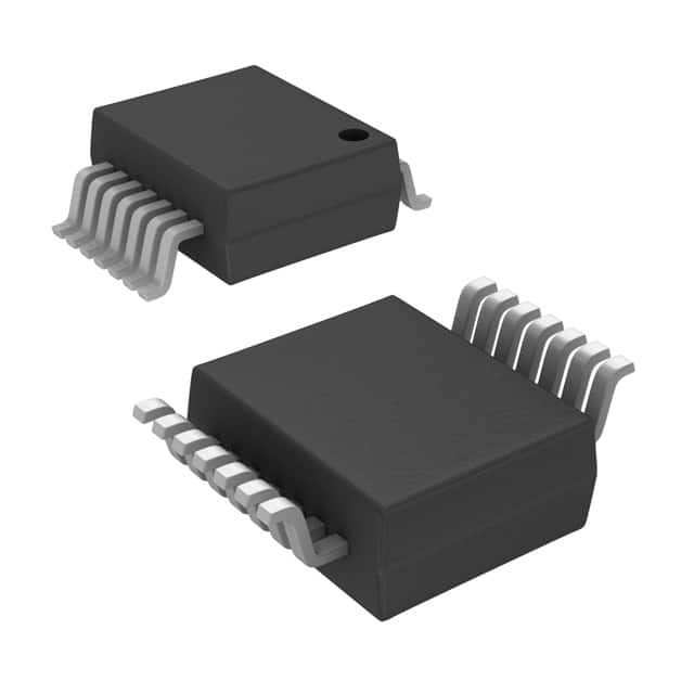
SN74LV139ADGVR is available in a small package, such as a TSSOP (Thin Shrink Small Outline Package).
Essence
The essence of SN74LV139ADGVR lies in its ability to decode and demultiplex signals efficiently and accurately.
Packaging/Quantity
This product is typically packaged in reels or tubes, with a quantity of 2500 units per reel/tube.
Specifications
- Supply Voltage: 2.0V to 5.5V
- Input Voltage: 0V to VCC
- Output Voltage: 0V to VCC
- Operating Temperature Range: -40°C to +85°C
- Logic Family: LV (Low Voltage)
- Number of Inputs: 2
- Number of Outputs: 4
Detailed Pin Configuration
SN74LV139ADGVR has a total of 16 pins, which are assigned specific functions as follows:
- GND: Ground pin
- A0: Input A0
- A1: Input A1
- Y0: Output Y0
- Y1: Output Y1
- Y2: Output Y2
- Y3: Output Y3
- VCC: Positive supply voltage pin
- GND: Ground pin
- B0: Input B0
- B1: Input B1
- Y4: Output Y4
- Y5: Output Y5
- Y6: Output Y6
- Y7: Output Y7
- VCC: Positive supply voltage pin
Functional Features
- Decodes and demultiplexes input signals based on the combination of A0 and A1 inputs.
- Provides four output lines (Y0 to Y3) for different combinations of input signals.
Advantages
- Low-voltage operation allows compatibility with a wide range of electronic devices.
- High-speed performance ensures efficient signal decoding and demultiplexing.
- Wide operating temperature range enables usage in various environmental conditions.
- Low power consumption contributes to energy efficiency.
Disadvantages
- Limited number of inputs and outputs may restrict its application in complex systems.
- Small package size may require careful handling during installation.
Working Principles
SN74LV139ADGVR works by receiving two input signals, A0 and A1, which determine the specific combination of outputs. The internal circuitry decodes these inputs and activates the corresponding output lines (Y0 to Y3). This allows the device to effectively demultiplex and distribute signals according to the desired configuration.
Detailed Application Field Plans
SN74LV139ADGVR finds applications in various fields, including but not limited to:
- Communication systems
- Data transmission equipment
- Digital multiplexers
- Address decoding circuits
- Control systems
Detailed and Complete Alternative Models
Some alternative models that can be considered as alternatives to SN74LV139ADGVR are:
- 74HC139: High-speed CMOS logic IC with similar functionality.
- CD74HC139E: Dual 2-to-4 line decoder/demultiplexer IC.
- MC74HC139AN: Dual 2-line to 4-line decoder/demultiplexer IC.
These alternative models offer comparable features and can be used as substitutes based on specific requirements.
Word count: 489 words
10 domande e risposte comuni relative all'applicazione di SN74LV139ADGVR nelle soluzioni tecniche
Sure! Here are 10 common questions and answers related to the application of SN74LV139ADGVR:
Q: What is SN74LV139ADGVR? A: SN74LV139ADGVR is a dual 2-to-4 line decoder/demultiplexer integrated circuit (IC) manufactured by Texas Instruments.
Q: What is the purpose of SN74LV139ADGVR? A: SN74LV139ADGVR is used to decode binary information from two input lines into four output lines, making it useful in various digital logic applications.
Q: What is the voltage range supported by SN74LV139ADGVR? A: SN74LV139ADGVR operates with a supply voltage range of 2 V to 5.5 V.
Q: How many input lines does SN74LV139ADGVR have? A: SN74LV139ADGVR has two input lines, labeled A0 and A1.
Q: How many output lines does SN74LV139ADGVR have? A: SN74LV139ADGVR has four output lines, labeled Y0, Y1, Y2, and Y3.
Q: Can SN74LV139ADGVR be cascaded to increase the number of decoded outputs? A: Yes, multiple SN74LV139ADGVR ICs can be cascaded together to increase the number of decoded outputs.
Q: What is the maximum operating frequency of SN74LV139ADGVR? A: SN74LV139ADGVR can operate at a maximum frequency of 50 MHz.
Q: Does SN74LV139ADGVR have any built-in protection features? A: Yes, SN74LV139ADGVR has built-in ESD (electrostatic discharge) protection on all inputs and outputs.
Q: What is the package type of SN74LV139ADGVR? A: SN74LV139ADGVR is available in a small SOT-23-6 package.
Q: What are some typical applications of SN74LV139ADGVR? A: SN74LV139ADGVR can be used in address decoding, data routing, memory selection, and other digital logic applications where binary information needs to be decoded into multiple outputs.
Please note that these answers are general and may vary depending on specific design requirements and application scenarios.