

Vedi le specifiche per i dettagli del prodotto.
SN74LV138ADGVR
Product Overview
- Category: Integrated Circuit (IC)
- Use: Decoder/Demultiplexer
- Characteristics: Low-voltage, 3-to-8 line decoder/demultiplexer
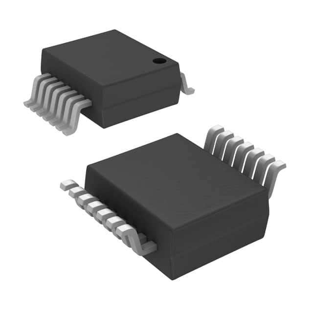
- Package: VSSOP (Very Small Outline Package)
- Essence: Converts binary information to a decoded output
- Packaging/Quantity: Tape and Reel, 2500 units per reel
Specifications
- Supply Voltage Range: 1.65V to 5.5V
- High-Level Input Voltage: 2V to VCC + 0.5V
- Low-Level Input Voltage: -0.5V to 0.8V
- High-Level Output Current: -12mA
- Low-Level Output Current: 12mA
- Operating Temperature Range: -40°C to 85°C
Detailed Pin Configuration
The SN74LV138ADGVR has a total of 16 pins. The pin configuration is as follows:
- GND (Ground)
- A0 (Address Input 0)
- A1 (Address Input 1)
- A2 (Address Input 2)
- /G1 (Enable Input)
- Y0 (Output 0)
- Y1 (Output 1)
- Y2 (Output 2)
- Y3 (Output 3)
- Y4 (Output 4)
- Y5 (Output 5)
- Y6 (Output 6)
- Y7 (Output 7)
- VCC (Positive Power Supply)
- /G2A (Enable Input)
- /G2B (Enable Input)
Functional Features
The SN74LV138ADGVR is a low-voltage decoder/demultiplexer IC that converts a 3-bit binary input into an 8-line output. It features three address inputs (A0, A1, and A2) that determine the selected output line based on the binary input. The /G1 enable input is used to activate the decoder/demultiplexer.
Advantages and Disadvantages
Advantages: - Low-voltage operation allows for compatibility with a wide range of systems - Compact VSSOP package saves board space - High-speed operation for efficient decoding
Disadvantages: - Limited to 3-bit input, restricting the number of output lines - Not suitable for applications requiring higher bit decoding
Working Principles
The SN74LV138ADGVR works by utilizing a combination of logic gates to decode the binary input and activate the corresponding output line. The address inputs determine which output line is enabled, while the enable inputs (/G1, /G2A, and /G2B) control the overall operation of the decoder/demultiplexer.
Detailed Application Field Plans
The SN74LV138ADGVR finds applications in various fields, including:
- Digital Electronics: Used in digital systems for address decoding and signal routing.
- Memory Systems: Enables selection of specific memory locations in RAM or ROM.
- Data Multiplexing: Facilitates data routing in communication systems.
- Control Systems: Allows for precise control of multiple devices based on address inputs.
Detailed and Complete Alternative Models
- SN74LS138: Similar 3-to-8 line decoder/demultiplexer with TTL-level inputs and outputs.
- CD74HC138: High-speed CMOS decoder/demultiplexer with similar functionality.
- 74HCT138: CMOS decoder/demultiplexer with Schmitt-trigger inputs for noise immunity.
These alternative models offer similar functionality to the SN74LV138ADGVR but may have different voltage levels, speed, or package options.
Word count: 345 words
10 domande e risposte comuni relative all'applicazione di SN74LV138ADGVR nelle soluzioni tecniche
Sure! Here are 10 common questions and answers related to the application of SN74LV138ADGVR:
Question: What is SN74LV138ADGVR?
- Answer: SN74LV138ADGVR is a 3-to-8 line decoder/demultiplexer integrated circuit (IC) that can be used in various technical solutions.Question: What is the purpose of SN74LV138ADGVR?
- Answer: The purpose of SN74LV138ADGVR is to decode binary information from input lines and activate the corresponding output line based on the input code.Question: What is the voltage range supported by SN74LV138ADGVR?
- Answer: SN74LV138ADGVR supports a voltage range of 2 V to 5.5 V.Question: How many input lines does SN74LV138ADGVR have?
- Answer: SN74LV138ADGVR has three input lines (A0, A1, and A2) for decoding purposes.Question: How many output lines does SN74LV138ADGVR have?
- Answer: SN74LV138ADGVR has eight output lines (Y0-Y7) that correspond to the decoded input code.Question: Can SN74LV138ADGVR be used as a demultiplexer?
- Answer: Yes, SN74LV138ADGVR can be used as a demultiplexer by connecting the input lines to the select lines and using the output lines as separate outputs.Question: What is the maximum current that SN74LV138ADGVR can sink/source per output?
- Answer: SN74LV138ADGVR can sink/source up to 24 mA per output.Question: Can SN74LV138ADGVR be cascaded to increase the number of decoded outputs?
- Answer: Yes, multiple SN74LV138ADGVR ICs can be cascaded together to increase the number of decoded outputs.Question: What is the typical propagation delay of SN74LV138ADGVR?
- Answer: The typical propagation delay of SN74LV138ADGVR is around 5 ns.Question: What are some common applications of SN74LV138ADGVR?
- Answer: SN74LV138ADGVR is commonly used in address decoding, memory selection, data routing, and general-purpose decoding applications.
Please note that these answers are general and may vary depending on specific use cases and requirements.