

Vedi le specifiche per i dettagli del prodotto.
SN74GTLP817DGVR
Product Overview
- Category: Integrated Circuit (IC)
- Use: Signal Level Translator
- Characteristics: Low-voltage, high-speed, dual-supply voltage translator
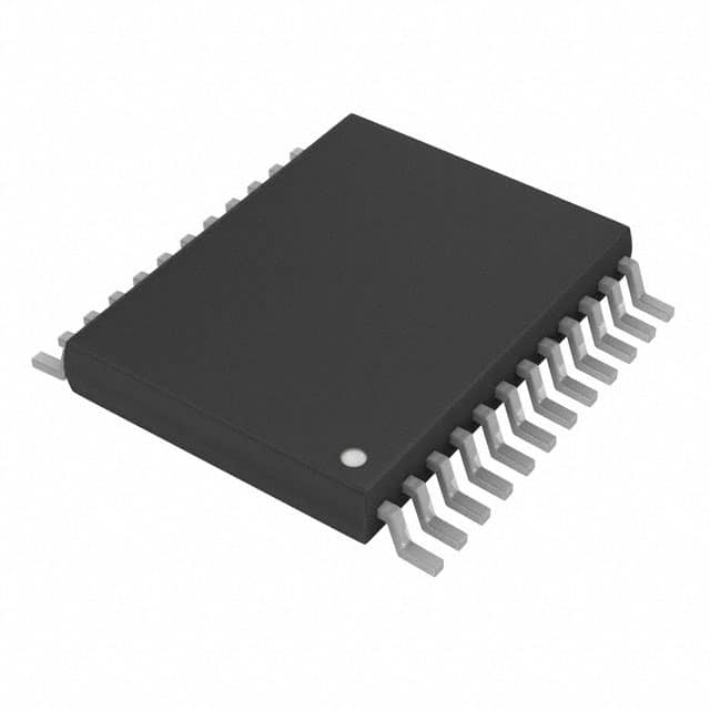
- Package: VSSOP (Very Small Outline Package)
- Essence: Translates signals between different voltage levels
- Packaging/Quantity: Tape and Reel, 2500 units per reel
Specifications
- Supply Voltage Range: 1.2V to 3.6V
- Input Voltage Range (A Port): 0V to VCCA + 0.5V
- Input Voltage Range (B Port): 0V to VCCB + 0.5V
- Output Voltage Range (A Port): 0V to VCCA + 0.5V
- Output Voltage Range (B Port): 0V to VCCB + 0.5V
- Maximum Data Rate: 100 Mbps
- Operating Temperature Range: -40°C to 85°C
Detailed Pin Configuration
The SN74GTLP817DGVR has a total of 16 pins:
- Pin 1: A1 (Input/Output)
- Pin 2: A2 (Input/Output)
- Pin 3: A3 (Input/Output)
- Pin 4: A4 (Input/Output)
- Pin 5: GND (Ground)
- Pin 6: B4 (Input/Output)
- Pin 7: B3 (Input/Output)
- Pin 8: B2 (Input/Output)
- Pin 9: B1 (Input/Output)
- Pin 10: VCCA (Supply Voltage for A Ports)
- Pin 11: OE (Output Enable)
- Pin 12: VCCB (Supply Voltage for B Ports)
- Pin 13: B5 (Input/Output)
- Pin 14: B6 (Input/Output)
- Pin 15: A6 (Input/Output)
- Pin 16: A5 (Input/Output)
Functional Features
- Dual-supply voltage translation between two different voltage domains
- Bidirectional level shifting for both input and output signals
- Supports high-speed data transmission up to 100 Mbps
- Low-voltage operation suitable for battery-powered devices
- Output enable pin for easy control of signal flow
Advantages and Disadvantages
Advantages: - Enables seamless communication between devices operating at different voltage levels - High-speed performance allows for efficient data transfer - Small package size saves board space - Wide supply voltage range provides flexibility in various applications
Disadvantages: - Limited maximum data rate compared to some other voltage translators - Not suitable for applications requiring very high voltage translation
Working Principles
The SN74GTLP817DGVR is designed to translate signals between two different voltage domains. It operates by using a combination of level shifters and voltage dividers to ensure proper signal compatibility. The device can handle bidirectional communication, allowing signals to be translated from one voltage level to another in both directions.
Detailed Application Field Plans
The SN74GTLP817DGVR is commonly used in various applications where voltage translation is required. Some of the typical application fields include:
- Mobile Devices: Used to interface between low-voltage components and higher-voltage peripherals.
- Industrial Automation: Facilitates communication between different voltage-level sensors and controllers.
- Automotive Electronics: Enables signal translation between various automotive systems operating at different voltage levels.
- Consumer Electronics: Allows for seamless integration of components with different voltage requirements, such as audio/video interfaces.
Detailed and Complete Alternative Models
- SN74LVC1T45DBVR: Single-bit dual-supply voltage translator with similar characteristics and package.
- SN74AVC4T245PWR: Four-bit dual-supply voltage translator with higher data rate capability.
- SN74LVC8T245PW: Eight-bit dual-supply voltage translator with wider supply voltage range.
These alternative models offer similar functionality to the SN74GTLP817DGVR but may have different specifications or package options.
Word count: 450 words
10 domande e risposte comuni relative all'applicazione di SN74GTLP817DGVR nelle soluzioni tecniche
Sure! Here are 10 common questions and answers related to the application of SN74GTLP817DGVR in technical solutions:
Q: What is the SN74GTLP817DGVR? A: The SN74GTLP817DGVR is a high-speed, low-power repeater/buffer IC designed for signal conditioning and amplification in various applications.
Q: What is the operating voltage range of SN74GTLP817DGVR? A: The operating voltage range of SN74GTLP817DGVR is typically between 1.2V and 3.6V.
Q: What is the maximum data rate supported by SN74GTLP817DGVR? A: SN74GTLP817DGVR supports data rates up to 2.5 Gbps, making it suitable for high-speed communication systems.
Q: Can SN74GTLP817DGVR be used as a level shifter? A: Yes, SN74GTLP817DGVR can be used as a level shifter to convert signals between different voltage levels.
Q: What is the typical propagation delay of SN74GTLP817DGVR? A: The typical propagation delay of SN74GTLP817DGVR is around 0.7 ns, ensuring fast signal transmission.
Q: Does SN74GTLP817DGVR have built-in ESD protection? A: Yes, SN74GTLP817DGVR features built-in ESD protection, safeguarding the IC from electrostatic discharge events.
Q: Can SN74GTLP817DGVR be used in both uni-directional and bi-directional applications? A: Yes, SN74GTLP817DGVR can be used in both uni-directional and bi-directional applications, providing flexibility in signal routing.
Q: What is the power supply current consumption of SN74GTLP817DGVR? A: The power supply current consumption of SN74GTLP817DGVR is typically around 10 mA, making it suitable for low-power applications.
Q: Is SN74GTLP817DGVR compatible with different logic families? A: Yes, SN74GTLP817DGVR is compatible with various logic families such as GTL, GTLP, and LVTTL, allowing seamless integration into existing systems.
Q: Can SN74GTLP817DGVR be used in high-temperature environments? A: Yes, SN74GTLP817DGVR has a wide operating temperature range of -40°C to 85°C, making it suitable for use in harsh conditions.
Please note that these answers are general and may vary depending on specific application requirements and datasheet specifications.