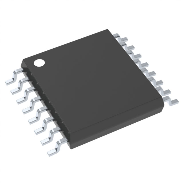
Vedi le specifiche per i dettagli del prodotto.

SN74AHC595QPWRQ1
Product Overview
Category
SN74AHC595QPWRQ1 belongs to the category of integrated circuits (ICs).
Use
It is commonly used as a shift register and output latches in various electronic devices.
Characteristics
- High-speed operation
- Low power consumption
- Wide operating voltage range
- Schmitt-trigger inputs for noise immunity
- Output current capability: 6 mA at VCC = 5 V
Package
SN74AHC595QPWRQ1 is available in a small-sized TSSOP package.
Essence
The essence of SN74AHC595QPWRQ1 lies in its ability to efficiently control multiple outputs using a minimal number of pins.
Packaging/Quantity
It is typically packaged in reels, with each reel containing a specific quantity of ICs.
Specifications
- Supply voltage range: 2 V to 5.5 V
- Operating temperature range: -40°C to +125°C
- Input voltage range: 0 V to VCC
- Output voltage range: 0 V to VCC
- Maximum clock frequency: 100 MHz
Detailed Pin Configuration
SN74AHC595QPWRQ1 has a total of 20 pins. The pin configuration is as follows:
- SER (Serial Data Input)
- RCLK (Register Clock Input)
- SRCLK (Shift Register Clock Input)
- OE (Output Enable Input)
- GND (Ground)
- QH' (Serial Data Output)
- QA (Parallel Data Output)
- QB (Parallel Data Output)
- QC (Parallel Data Output)
- QD (Parallel Data Output)
- QE (Parallel Data Output)
- QF (Parallel Data Output)
- QG (Parallel Data Output)
- QH (Parallel Data Output)
- VCC (Supply Voltage)
Functional Features
- Serial-to-parallel data conversion
- Cascading capability for expanding the number of outputs
- Output latching for stable data retention
- Output enable control for power-saving mode
Advantages and Disadvantages
Advantages
- High-speed operation allows for efficient data transfer
- Low power consumption helps in reducing energy usage
- Wide operating voltage range provides flexibility in various applications
- Schmitt-trigger inputs ensure reliable operation in noisy environments
Disadvantages
- Limited output current capability may restrict certain high-power applications
- TSSOP package may require careful handling during assembly
Working Principles
SN74AHC595QPWRQ1 operates based on the shift register principle. It receives serial data input (SER) and shifts it through the internal shift register upon receiving a clock signal (SRCLK). The parallel data is then latched into the output registers upon receiving another clock signal (RCLK). The latched data is available at the parallel output pins (QA-QH).
Detailed Application Field Plans
SN74AHC595QPWRQ1 finds applications in various fields, including but not limited to: - LED matrix displays - Seven-segment displays - Multiplexed LED indicators - Control panels with multiple buttons/switches - Data storage and retrieval systems
Detailed and Complete Alternative Models
Some alternative models that can be considered as alternatives to SN74AHC595QPWRQ1 are: - 74HC595 - CD4094 - TPIC6B595 - STP16C596
These models offer similar functionality and can be used as replacements depending on specific requirements.
Word count: 476 words
10 domande e risposte comuni relative all'applicazione di SN74AHC595QPWRQ1 nelle soluzioni tecniche
Sure! Here are 10 common questions and answers related to the application of SN74AHC595QPWRQ1 in technical solutions:
1. What is the SN74AHC595QPWRQ1? - The SN74AHC595QPWRQ1 is a shift register with output latches that can be used to expand the number of outputs in a microcontroller or other digital system.
2. What is the maximum operating voltage for SN74AHC595QPWRQ1? - The maximum operating voltage for SN74AHC595QPWRQ1 is 5.5V.
3. How many outputs does SN74AHC595QPWRQ1 have? - SN74AHC595QPWRQ1 has 8 outputs.
4. Can SN74AHC595QPWRQ1 be cascaded to increase the number of outputs? - Yes, SN74AHC595QPWRQ1 can be cascaded to increase the number of outputs by connecting the serial output of one shift register to the serial input of another.
5. What is the maximum clock frequency for SN74AHC595QPWRQ1? - The maximum clock frequency for SN74AHC595QPWRQ1 is typically 100 MHz.
6. Can SN74AHC595QPWRQ1 be used with both CMOS and TTL logic levels? - Yes, SN74AHC595QPWRQ1 is compatible with both CMOS and TTL logic levels.
7. What is the power supply voltage range for SN74AHC595QPWRQ1? - The power supply voltage range for SN74AHC595QPWRQ1 is 2V to 5.5V.
8. Does SN74AHC595QPWRQ1 have built-in protection against electrostatic discharge (ESD)? - Yes, SN74AHC595QPWRQ1 has built-in ESD protection.
9. Can SN74AHC595QPWRQ1 be used in automotive applications? - Yes, SN74AHC595QPWRQ1 is specifically designed for automotive applications and meets the AEC-Q100 automotive qualification standards.
10. What is the package type for SN74AHC595QPWRQ1? - SN74AHC595QPWRQ1 comes in a TSSOP-16 package.
Please note that these answers are general and may vary depending on the specific datasheet and application requirements.

