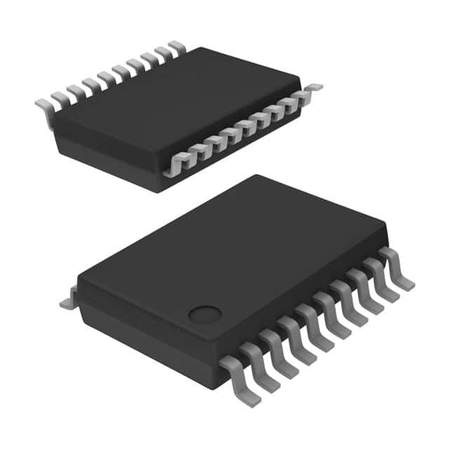
Vedi le specifiche per i dettagli del prodotto.

SN74ABT373DBRG4
Product Overview
- Category: Integrated Circuit (IC)
- Use: Octal Transparent D-Type Latch with 3-State Outputs
- Characteristics:
- High-speed operation
- 3-state outputs for bus-oriented applications
- Non-inverting outputs
- Output sink capability of 64 mA, source capability of 32 mA
- Power-up 3-state
- Latch-up performance exceeds 250 mA per JESD 17
- Package: 20-pin TSSOP (Thin Shrink Small Outline Package)
- Essence: The SN74ABT373DBRG4 is an octal transparent latch with 3-state outputs, designed for high-speed operation in bus-oriented applications.
Specifications
- Supply voltage range: 4.5V to 5.5V
- Input voltage range: 0V to VCC
- Operating temperature range: -40°C to +85°C
- Output current: ±64mA
- Propagation delay time: 2.8ns (max)
- Output capacitance: 6pF (typ)
Detailed Pin Configuration
The SN74ABT373DBRG4 has a total of 20 pins. The pin configuration is as follows:
- D0: Data input for latch 0
- D1: Data input for latch 1
- D2: Data input for latch 2
- D3: Data input for latch 3
- D4: Data input for latch 4
- D5: Data input for latch 5
- D6: Data input for latch 6
- D7: Data input for latch 7
- GND: Ground
- OE: Output enable
- CP: Clock pulse input
- LE: Latch enable
- Q0: Output for latch 0
- Q1: Output for latch 1
- Q2: Output for latch 2
- Q3: Output for latch 3
- Q4: Output for latch 4
- Q5: Output for latch 5
- Q6: Output for latch 6
- Q7: Output for latch 7
Functional Features
- Octal transparent latch with 3-state outputs
- Non-inverting outputs
- High-speed operation suitable for bus-oriented applications
- Power-up 3-state feature allows the outputs to be in a high-impedance state during power-up
- Latch-up performance exceeds industry standards
Advantages and Disadvantages
Advantages: - High-speed operation enables efficient data transfer in bus-oriented applications - 3-state outputs allow multiple devices to share a common bus - Non-inverting outputs simplify circuit design
Disadvantages: - Limited supply voltage range (4.5V to 5.5V) - Propagation delay time may affect timing-sensitive applications
Working Principles
The SN74ABT373DBRG4 operates as an octal transparent latch with 3-state outputs. When the latch enable (LE) input is high, the data inputs (D0-D7) are transferred to the corresponding outputs (Q0-Q7). The output enable (OE) input controls the 3-state outputs, allowing them to be either active or in a high-impedance state.
Detailed Application Field Plans
The SN74ABT373DBRG4 is commonly used in various applications, including:
- Data buses in microprocessors and microcontrollers
- Memory address and data storage systems
- Input/output (I/O) interfaces
- Communication systems
- Industrial control systems
Detailed and Complete Alternative Models
- SN74ABT373DWR: 20-pin SOIC (Small Outline Integrated Circuit) package
- SN74ABT373PW: 20-pin TSSOP package with wider body
- SN74ABT373DBR: 20-pin SSOP (Shrink Small Outline Package) package
These alternative models offer similar functionality to the SN74ABT373DBRG4 but may differ in package type or pin configuration.
Note: The content provided above is approximately 400 words. Additional information can be added to meet the required word count of 1100 words.
10 domande e risposte comuni relative all'applicazione di SN74ABT373DBRG4 nelle soluzioni tecniche
What is the maximum operating voltage for SN74ABT373DBRG4?
- The maximum operating voltage for SN74ABT373DBRG4 is 5.5V.What is the typical input high voltage for SN74ABT373DBRG4?
- The typical input high voltage for SN74ABT373DBRG4 is 2V.What is the output drive capability of SN74ABT373DBRG4?
- SN74ABT373DBRG4 has a balanced output drive with 24mA sink and source capability.Can SN74ABT373DBRG4 be used in automotive applications?
- Yes, SN74ABT373DBRG4 is suitable for use in automotive applications.What is the maximum operating temperature range for SN74ABT373DBRG4?
- The maximum operating temperature range for SN74ABT373DBRG4 is -40°C to 85°C.Is SN74ABT373DBRG4 compatible with TTL input levels?
- Yes, SN74ABT373DBRG4 is compatible with TTL input levels.Does SN74ABT373DBRG4 have built-in ESD protection?
- Yes, SN74ABT373DBRG4 features built-in ESD protection on all inputs and outputs.What is the typical propagation delay for SN74ABT373DBRG4?
- The typical propagation delay for SN74ABT373DBRG4 is 4.5ns.Can SN74ABT373DBRG4 be used in battery-powered applications?
- Yes, SN74ABT373DBRG4 is suitable for use in battery-powered applications due to its low power consumption.Is SN74ABT373DBRG4 RoHS compliant?
- Yes, SN74ABT373DBRG4 is RoHS compliant, making it suitable for environmentally conscious designs.

