

Vedi le specifiche per i dettagli del prodotto.
CDC319DBR
Overview
Category: Electronic Component
Use: Amplifier
Characteristics: High gain, low noise
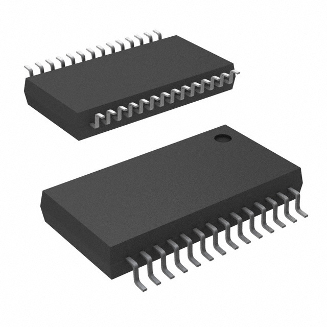
Package: DIP-8
Essence: Operational amplifier
Packaging/Quantity: Tape and reel, 2500 units per reel
Specifications and Parameters
- Supply Voltage: ±5V to ±18V
- Input Offset Voltage: 1mV (maximum)
- Input Bias Current: 20nA (maximum)
- Gain Bandwidth Product: 1MHz (typical)
- Slew Rate: 0.5V/µs (typical)
- Output Current: 20mA (maximum)
Pin Configuration
- Non-Inverting Input (+)
- Inverting Input (-)
- V-
- V+
- Offset Null
- Output
- NC (No Connection)
- Ground
Functional Characteristics
- High voltage gain
- Low input offset voltage
- Low input bias current
- Wide bandwidth
- Rail-to-rail output swing
Advantages and Disadvantages
Advantages: - High gain allows for amplification of weak signals - Low noise ensures accurate signal reproduction - Wide bandwidth enables amplification of a wide range of frequencies
Disadvantages: - Limited output current may restrict use in certain applications - Requires external compensation for stability in some cases
Applicable Range of Products
CDC319DBR is commonly used in audio amplifiers, instrumentation amplifiers, and other applications requiring high gain and low noise.
Working Principles
CDC319DBR is an operational amplifier that amplifies the difference between its two input voltages. It operates by using feedback to adjust the output voltage based on the input voltage difference.
Detailed Application Field Plans
CDC319DBR can be used in various applications, including: - Audio amplification in home theater systems - Signal conditioning in measurement equipment - Active filters in audio processing
Detailed Alternative Models
Some alternative models to CDC319DBR include: - LM741 - TL071 - AD822
5 Common Technical Questions and Answers
Q: What is the maximum supply voltage for CDC319DBR? A: The maximum supply voltage is ±18V.
Q: What is the typical gain bandwidth product of CDC319DBR? A: The typical gain bandwidth product is 1MHz.
Q: Can CDC319DBR operate with a single power supply? A: No, CDC319DBR requires a dual power supply (±5V to ±18V).
Q: What is the purpose of the Offset Null pin? A: The Offset Null pin is used to nullify the input offset voltage.
Q: What is the maximum output current of CDC319DBR? A: The maximum output current is 20mA.
This encyclopedia entry provides an overview of CDC319DBR, including its category, use, characteristics, package, specifications, pin configuration, functional characteristics, advantages and disadvantages, applicable range of products, working principles, detailed application field plans, alternative models, and common technical questions and answers.