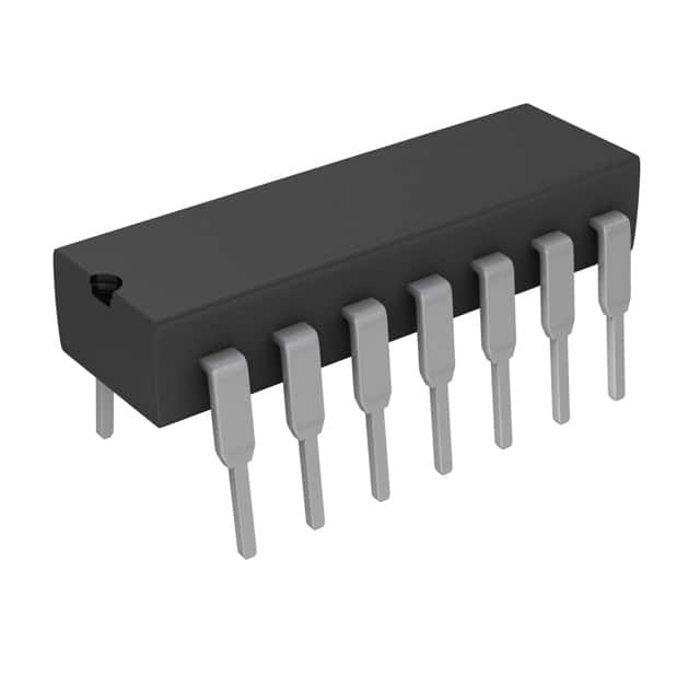
Vedi le specifiche per i dettagli del prodotto.

CD4001BE
Product Overview
- Category: Integrated Circuit (IC)
- Use: Logic Gate
- Characteristics: Quad 2-input NOR gate
- Package: PDIP-14 (Plastic Dual In-line Package)
- Essence: Digital logic gate
- Packaging/Quantity: Tube/25 pieces
Specifications
- Supply Voltage Range: 3V to 18V
- Input Voltage Range: 0V to VDD
- Output Voltage Range: 0V to VDD
- Operating Temperature Range: -55°C to +125°C
- Propagation Delay Time: 60ns (typical)
Detailed Pin Configuration
The CD4001BE IC has a total of 14 pins, numbered as follows:
```
| | | 1 2 3 4 5 6 7 8 | | | | 9 10 11 12 13 14 | | |
```
Pin Description: 1. A Input 1 2. B Input 1 3. Y Output 1 4. A Input 2 5. B Input 2 6. Y Output 2 7. GND (Ground) 8. C Input 1 9. D Input 1 10. Y Output 3 11. C Input 2 12. D Input 2 13. Y Output 4 14. VDD (Supply Voltage)
Functional Features
The CD4001BE is a quad 2-input NOR gate integrated circuit. It is designed to perform logical NOR operations on two input signals. The output is the logical complement of the OR function. The IC operates over a wide range of supply voltages and is compatible with both TTL and CMOS logic levels.
Advantages and Disadvantages
Advantages: - High noise immunity - Wide supply voltage range - Compatible with various logic families - Low power consumption
Disadvantages: - Limited number of inputs and outputs - Propagation delay may affect timing-sensitive applications
Working Principles
The CD4001BE consists of four independent NOR gates, each having two inputs and one output. The gate operates by comparing the logical states of its input signals and producing an output based on the NOR function. When both inputs are low (logic 0), the output becomes high (logic 1). In all other cases, the output remains low.
Detailed Application Field Plans
The CD4001BE is commonly used in various digital logic applications, including:
- Logic circuit design
- Data processing systems
- Arithmetic circuits
- Control systems
- Signal conditioning circuits
Detailed and Complete Alternative Models
Some alternative models to the CD4001BE include:
- CD4001BCN: Same functionality, different package (DIP-14)
- MC14001B: Equivalent functionality from a different manufacturer (Motorola)
- SN74LS02: Similar functionality, but with different electrical characteristics (TTL logic)
These alternative models can be used as replacements for the CD4001BE depending on specific requirements and availability.
Word count: 345 words
10 domande e risposte comuni relative all'applicazione di CD4001BE nelle soluzioni tecniche
Sure! Here are 10 common questions and answers related to the application of CD4001BE in technical solutions:
Q: What is CD4001BE? A: CD4001BE is a quad 2-input NOR gate integrated circuit (IC) commonly used in digital logic circuits.
Q: What is the purpose of CD4001BE? A: CD4001BE is used to perform logical NOR operations in various electronic applications.
Q: How many inputs does CD4001BE have? A: CD4001BE has four inputs, allowing it to process multiple signals simultaneously.
Q: What is the voltage range supported by CD4001BE? A: CD4001BE operates within a voltage range of 3V to 18V, making it compatible with a wide range of power supplies.
Q: Can CD4001BE be used as an inverter? A: Yes, CD4001BE can be used as an inverter by connecting both inputs together and using it as a NOT gate.
Q: How can CD4001BE be used in combination with other ICs? A: CD4001BE can be cascaded with other ICs to create more complex logic functions or build larger digital systems.
Q: What is the maximum current that CD4001BE can source or sink? A: CD4001BE can source or sink up to 2.5mA of current per output pin.
Q: Can CD4001BE operate at high frequencies? A: CD4001BE is not designed for high-frequency applications and is typically used in low to moderate speed digital circuits.
Q: Is CD4001BE sensitive to electrostatic discharge (ESD)? A: Yes, CD4001BE is sensitive to ESD and should be handled with proper ESD precautions to avoid damage.
Q: What are some common applications of CD4001BE? A: CD4001BE is commonly used in applications such as logic gates, flip-flops, counters, multiplexers, and various digital systems.
Please note that these answers are general and may vary depending on specific circuit designs and requirements.

