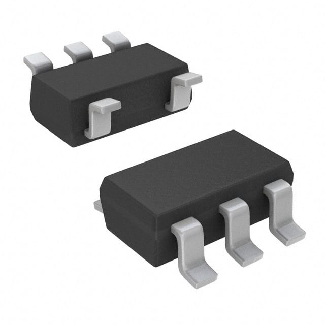
Vedi le specifiche per i dettagli del prodotto.

Encyclopedia Entry: 74AUC1G125DCKRE4
Product Information Overview
Category
The 74AUC1G125DCKRE4 belongs to the category of integrated circuits (ICs).
Use
This IC is commonly used as a buffer or line driver in various electronic devices and systems.
Characteristics
- Low power consumption
- High-speed operation
- Wide operating voltage range
- Small package size
- RoHS compliant
Package
The 74AUC1G125DCKRE4 is available in a small SOT-353 package.
Essence
The essence of this IC lies in its ability to provide signal buffering and driving capabilities, ensuring reliable and efficient data transmission within electronic circuits.
Packaging/Quantity
The 74AUC1G125DCKRE4 is typically packaged in reels containing a quantity of 3000 units.
Specifications
- Supply Voltage Range: 0.8V to 3.6V
- Input Voltage Range: -0.5V to VCC + 0.5V
- Output Voltage Range: -0.5V to VCC + 0.5V
- Operating Temperature Range: -40°C to +85°C
- Maximum Propagation Delay: 2.9ns (typical)
- Maximum Quiescent Current: 10μA (typical)
Detailed Pin Configuration
The 74AUC1G125DCKRE4 has the following pin configuration:
____
   Y ---|    |
   A ---|    |
   GND -|    |
   OE --|    |
   VCC -|    |
         ----
Functional Features
- Single gate buffer with tri-state output
- Non-inverting logic function
- High-speed data transmission
- Low power consumption
- ESD protection on all inputs and outputs
Advantages and Disadvantages
Advantages
- Small package size allows for space-efficient designs
- Wide operating voltage range enables compatibility with various systems
- Low power consumption contributes to energy efficiency
- High-speed operation ensures fast data transmission
Disadvantages
- Limited output current capability
- Single gate functionality may not be suitable for complex circuit requirements
Working Principles
The 74AUC1G125DCKRE4 operates by receiving an input signal at the A pin, which is then buffered and amplified. The resulting output signal appears at the Y pin. The OE (Output Enable) pin controls the tri-state output, allowing the IC to be enabled or disabled as needed.
Detailed Application Field Plans
The 74AUC1G125DCKRE4 finds applications in various electronic devices and systems, including but not limited to: - Mobile phones - Tablets - Portable media players - Digital cameras - Automotive electronics - Industrial control systems
Detailed and Complete Alternative Models
Some alternative models that offer similar functionality to the 74AUC1G125DCKRE4 include: - SN74LVC1G125DBVR - MC74VHC1G125DTT1G - TC7SZ125FU
These alternatives can be considered based on specific design requirements and availability.
Word count: 410 words
10 domande e risposte comuni relative all'applicazione di 74AUC1G125DCKRE4 nelle soluzioni tecniche
Sure! Here are 10 common questions and answers related to the application of 74AUC1G125DCKRE4 in technical solutions:
Q1: What is the 74AUC1G125DCKRE4? A1: The 74AUC1G125DCKRE4 is a single bus buffer gate with 3-state output. It is commonly used in digital logic circuits.
Q2: What is the operating voltage range for 74AUC1G125DCKRE4? A2: The operating voltage range for 74AUC1G125DCKRE4 is typically between 0.8V and 3.6V.
Q3: What is the maximum output current of 74AUC1G125DCKRE4? A3: The maximum output current of 74AUC1G125DCKRE4 is typically around 32mA.
Q4: Can 74AUC1G125DCKRE4 be used as a level shifter? A4: Yes, 74AUC1G125DCKRE4 can be used as a level shifter to convert signals from one voltage level to another.
Q5: What is the propagation delay of 74AUC1G125DCKRE4? A5: The propagation delay of 74AUC1G125DCKRE4 is typically around 2.5ns.
Q6: Can 74AUC1G125DCKRE4 drive capacitive loads? A6: Yes, 74AUC1G125DCKRE4 can drive small capacitive loads without any additional buffering.
Q7: Is 74AUC1G125DCKRE4 suitable for high-speed applications? A7: Yes, 74AUC1G125DCKRE4 is designed for high-speed applications and can operate at frequencies up to several hundred megahertz.
Q8: Can 74AUC1G125DCKRE4 be used in battery-powered devices? A8: Yes, 74AUC1G125DCKRE4 is suitable for battery-powered devices as it operates at low voltage levels.
Q9: What is the package type of 74AUC1G125DCKRE4? A9: 74AUC1G125DCKRE4 is available in a small SOT-353 package.
Q10: Can multiple 74AUC1G125DCKRE4 gates be cascaded together? A10: Yes, multiple 74AUC1G125DCKRE4 gates can be cascaded together to achieve more complex logic functions.
Please note that the answers provided here are general and may vary depending on specific datasheet specifications or application requirements.

