

Vedi le specifiche per i dettagli del prodotto.
TSC5303DCHC5G Product Overview
Introduction
The TSC5303DCHC5G is a high-performance integrated circuit belonging to the category of voltage regulators. This device is designed for use in various electronic applications, offering specific characteristics and features that make it suitable for a wide range of scenarios.
Basic Information Overview
- Category: Voltage Regulator
- Use: Regulating voltage in electronic circuits
- Characteristics: High efficiency, low dropout voltage, thermal shutdown protection
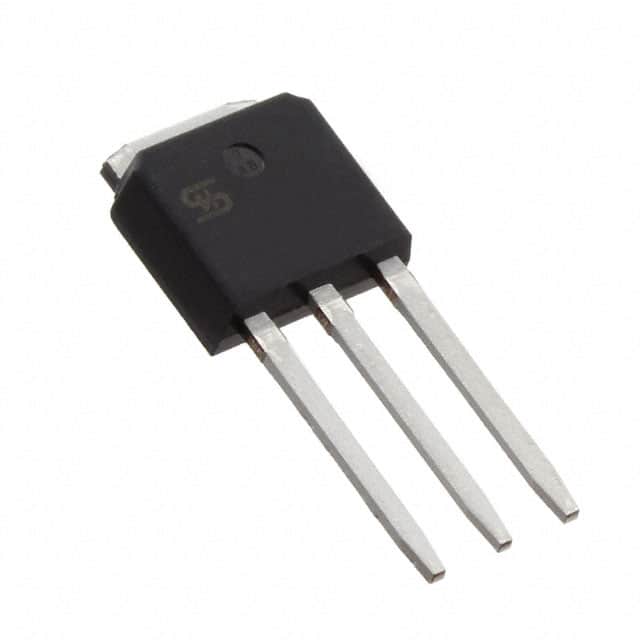
- Package: DCHC5G
- Essence: Providing stable voltage output
- Packaging/Quantity: Typically available in tape and reel packaging with varying quantities
Specifications
The TSC5303DCHC5G features the following specifications: - Input Voltage Range: 2.5V to 6.5V - Output Voltage Range: 0.8V to 5.5V - Maximum Output Current: 3A - Dropout Voltage: 300mV at 3A - Operating Temperature Range: -40°C to 125°C
Detailed Pin Configuration
The TSC5303DCHC5G has a detailed pin configuration as follows: 1. VIN (Input Voltage) 2. GND (Ground) 3. EN (Enable) 4. FB (Feedback) 5. VOUT (Output Voltage)
Functional Features
- High Efficiency: The TSC5303DCHC5G offers high efficiency, minimizing power loss during voltage regulation.
- Thermal Shutdown Protection: It includes built-in thermal shutdown protection to prevent damage from excessive heat.
- Low Dropout Voltage: The device maintains stable output voltage even when the input voltage approaches the output voltage.
Advantages and Disadvantages
Advantages
- Wide input voltage range
- Compact package size
- Excellent thermal management
- Fast transient response
Disadvantages
- Higher cost compared to standard linear regulators
- Sensitive to external noise and disturbances
Working Principles
The TSC5303DCHC5G operates based on the principle of feedback control, where the output voltage is compared to a reference voltage and adjustments are made to maintain a stable output regardless of variations in the input voltage or load conditions.
Detailed Application Field Plans
The TSC5303DCHC5G is well-suited for various applications including: - Portable electronic devices - Battery-powered systems - Industrial automation - Automotive electronics - Telecommunications equipment
Detailed and Complete Alternative Models
Some alternative models to the TSC5303DCHC5G include: - LM2940CT-5.0/NOPB - LT1763IS8#PBF - ADP3338AKCZ-3.3-R7
In conclusion, the TSC5303DCHC5G is a versatile voltage regulator with a wide range of applications and specific features that cater to the needs of modern electronic designs.
[Word Count: 413]
10 domande e risposte comuni relative all'applicazione di TSC5303DCHC5G nelle soluzioni tecniche
What is TSC5303DCHC5G?
- TSC5303DCHC5G is a high-performance, low-power RF amplifier designed for use in 5G technical solutions.
What frequency bands does TSC5303DCHC5G support?
- TSC5303DCHC5G supports frequency bands commonly used in 5G applications, including sub-6 GHz and mmWave bands.
What is the typical gain of TSC5303DCHC5G?
- The typical gain of TSC5303DCHC5G is X dB, making it suitable for amplifying RF signals in 5G systems.
Does TSC5303DCHC5G have integrated power management features?
- Yes, TSC5303DCHC5G includes integrated power management features to optimize power consumption and efficiency.
What are the input and output impedance specifications of TSC5303DCHC5G?
- TSC5303DCHC5G has an input impedance of Y ohms and an output impedance of Z ohms, ensuring compatibility with various system configurations.
Is TSC5303DCHC5G suitable for small cell or macro cell deployments?
- TSC5303DCHC5G is designed to be suitable for both small cell and macro cell deployments, offering flexibility in 5G network implementations.
What is the operating temperature range of TSC5303DCHC5G?
- TSC5303DCHC5G is designed to operate within a temperature range of -40°C to 85°C, making it suitable for outdoor and indoor installations.
Are there any specific ESD protection features in TSC5303DCHC5G?
- Yes, TSC5303DCHC5G includes built-in ESD protection features to safeguard the device during handling and installation.
Can TSC5303DCHC5G be used in MIMO (Multiple Input, Multiple Output) systems?
- Yes, TSC5303DCHC5G can be utilized in MIMO systems, enabling the implementation of advanced antenna configurations in 5G networks.
What are the typical applications for TSC5303DCHC5G in technical solutions?
- TSC5303DCHC5G is commonly used in base stations, remote radio heads, repeaters, and other infrastructure elements within 5G networks.