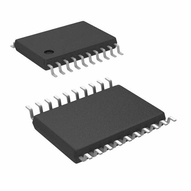
Vedi le specifiche per i dettagli del prodotto.

74LVQ373TTR
Product Overview
- Category: Integrated Circuit (IC)
- Use: Data storage and transfer
- Characteristics: High-speed, low-voltage, transparent latch
- Package: TSSOP (Thin Shrink Small Outline Package)
- Essence: Transparent latch with eight D-type flip-flops
- Packaging/Quantity: Tape and reel, 2500 units per reel
Specifications
- Supply Voltage Range: 1.65V to 5.5V
- High-Level Input Voltage: 2V to VCC + 0.3V
- Low-Level Input Voltage: -0.3V to 0.8V
- High-Level Output Voltage: VCC - 0.3V
- Low-Level Output Voltage: 0.3V
- Maximum Operating Frequency: 200MHz
- Propagation Delay Time: 4.6ns (typical)
Detailed Pin Configuration
The 74LVQ373TTR IC has a total of 20 pins, which are assigned as follows:
- OE (Output Enable) - Output control pin
- D0-D7 (Data Inputs) - Eight data input pins
- Q0-Q7 (Data Outputs) - Eight data output pins
- GND (Ground) - Ground reference
- LE (Latch Enable) - Latch enable pin
- VCC (Supply Voltage) - Positive supply voltage
Functional Features
- Transparent latch operation
- Non-inverting outputs
- High-speed data transfer
- Low power consumption
- Wide operating voltage range
- Schmitt-trigger inputs for noise immunity
Advantages and Disadvantages
Advantages: - High-speed operation allows for efficient data transfer. - Low-voltage operation reduces power consumption. - Transparent latch enables real-time data storage and retrieval. - Schmitt-trigger inputs provide noise immunity.
Disadvantages: - Limited number of data inputs and outputs (8 each). - Propagation delay may affect timing-sensitive applications. - TSSOP package may require careful handling during assembly.
Working Principles
The 74LVQ373TTR is a transparent latch that stores and transfers data. When the latch enable (LE) pin is high, the data inputs (D0-D7) are transferred to the corresponding data outputs (Q0-Q7). The output enable (OE) pin controls the state of the outputs. When OE is low, the outputs are active; when OE is high, the outputs are in a high-impedance state.
Detailed Application Field Plans
The 74LVQ373TTR IC finds applications in various fields, including:
- Data storage systems
- Communication devices
- Microcontrollers
- Networking equipment
- Industrial automation
- Automotive electronics
Detailed and Complete Alternative Models
Some alternative models to the 74LVQ373TTR IC include:
- 74HC373: Similar latch with higher voltage tolerance
- 74LS373: TTL logic family equivalent with different characteristics
- SN74LVC373: Low-voltage CMOS latch with similar features
- CD74ACT373: Advanced CMOS latch with faster operation
These alternative models offer different specifications and characteristics, allowing users to choose the most suitable option for their specific requirements.
Word count: 366 words
10 domande e risposte comuni relative all'applicazione di 74LVQ373TTR nelle soluzioni tecniche
Sure! Here are 10 common questions and answers related to the application of 74LVQ373TTR in technical solutions:
Question: What is the 74LVQ373TTR?
- Answer: The 74LVQ373TTR is a transparent latch with 3-state outputs, commonly used in digital circuits.Question: What is the purpose of using the 74LVQ373TTR in a technical solution?
- Answer: The 74LVQ373TTR is used to store and control the flow of data in digital systems, making it useful for applications such as memory interfacing and bus control.Question: What voltage levels does the 74LVQ373TTR support?
- Answer: The 74LVQ373TTR supports a wide range of voltage levels, typically ranging from 2V to 5.5V.Question: Can the 74LVQ373TTR be used in both synchronous and asynchronous systems?
- Answer: Yes, the 74LVQ373TTR can be used in both synchronous and asynchronous systems, depending on the specific requirements of the application.Question: How many latch outputs does the 74LVQ373TTR have?
- Answer: The 74LVQ373TTR has 8 latch outputs, which can be individually controlled.Question: What is the maximum operating frequency of the 74LVQ373TTR?
- Answer: The maximum operating frequency of the 74LVQ373TTR is typically around 200 MHz, making it suitable for high-speed applications.Question: Can the 74LVQ373TTR be cascaded to increase the number of latch outputs?
- Answer: Yes, multiple 74LVQ373TTRs can be cascaded together to increase the number of latch outputs, allowing for larger data storage and control.Question: Does the 74LVQ373TTR have built-in protection against electrostatic discharge (ESD)?
- Answer: Yes, the 74LVQ373TTR typically includes built-in ESD protection, ensuring its reliability in various environments.Question: Can the 74LVQ373TTR operate in a wide temperature range?
- Answer: Yes, the 74LVQ373TTR is designed to operate in a wide temperature range, typically from -40°C to 85°C.Question: Are there any specific application notes or reference designs available for the 74LVQ373TTR?
- Answer: Yes, the manufacturer of the 74LVQ373TTR usually provides application notes and reference designs that can help users understand and implement the chip in their technical solutions.
Please note that the answers provided here are general and may vary depending on the specific datasheet and manufacturer's documentation for the 74LVQ373TTR.

