

Vedi le specifiche per i dettagli del prodotto.
SLA5201 Product Overview
Introduction
The SLA5201 is a versatile integrated circuit that belongs to the category of power management ICs. This device is widely used in various electronic applications due to its unique characteristics and functional features. In this entry, we will provide an overview of the SLA5201, including its basic information, specifications, pin configuration, functional features, advantages and disadvantages, working principles, application field plans, and alternative models.
Basic Information Overview
- Category: Power Management IC
- Use: Voltage Regulator
- Characteristics: High efficiency, low dropout voltage, thermal shutdown protection
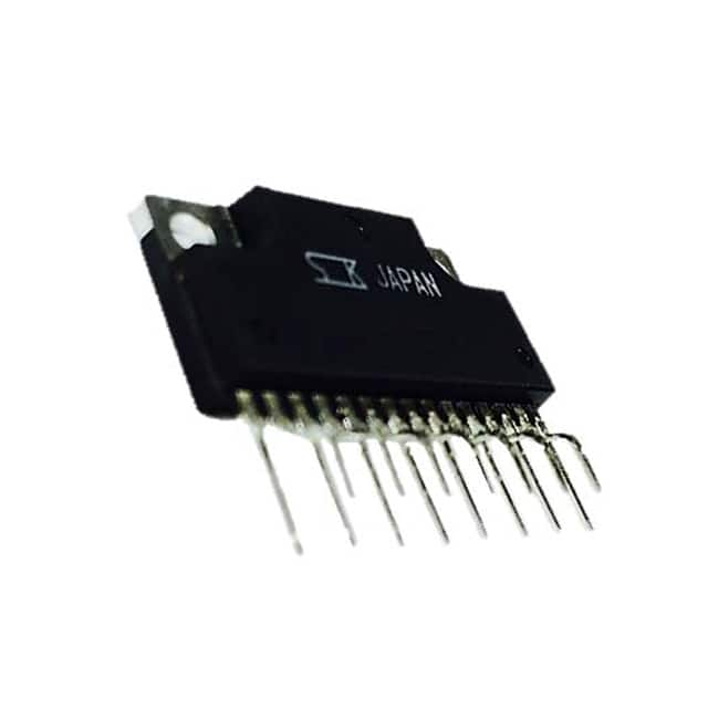
- Package: TO-220, TO-263
- Essence: Regulating voltage for electronic devices
- Packaging/Quantity: Typically available in reels or tubes containing multiple units
Specifications
- Input Voltage Range: 4.5V to 40V
- Output Voltage Range: 1.2V to 37V
- Output Current: Up to 3A
- Dropout Voltage: 1.5V at 3A
- Operating Temperature Range: -40°C to 125°C
Detailed Pin Configuration
The SLA5201 typically consists of multiple pins, including input, output, ground, and enable pins. The specific pin configuration can be found in the product datasheet provided by the manufacturer.
Functional Features
- Voltage Regulation: Provides stable output voltage despite fluctuations in input voltage
- Thermal Shutdown Protection: Prevents the IC from overheating
- Current Limiting: Protects the circuit from excessive current flow
Advantages and Disadvantages
Advantages
- High efficiency
- Wide input voltage range
- Thermal shutdown protection
Disadvantages
- Higher dropout voltage compared to some alternative models
- Limited maximum output current
Working Principles
The SLA5201 operates based on the principle of feedback control, where it compares the actual output voltage with a reference voltage and adjusts the output to maintain a stable voltage level. It utilizes internal circuitry to regulate the output voltage and protect the device from overcurrent and overheating.
Detailed Application Field Plans
The SLA5201 finds extensive use in various applications, including: - Automotive electronics - Industrial power supplies - Consumer electronics - Telecommunications equipment
Detailed and Complete Alternative Models
- SLA5200: Similar specifications with a lower dropout voltage
- SLA5202: Higher output current capability with slightly different package options
In conclusion, the SLA5201 is a reliable and efficient power management IC with a wide range of applications. Its high efficiency, thermal protection, and wide input voltage range make it a popular choice for voltage regulation in diverse electronic devices.
Word Count: 410
10 domande e risposte comuni relative all'applicazione di SLA5201 nelle soluzioni tecniche
What is SLA5201?
- SLA5201 is a high-performance, low-power audio amplifier designed for use in various technical solutions.
What is the typical application of SLA5201?
- The typical application of SLA5201 includes use in portable devices, automotive audio systems, and home entertainment systems.
What is the power rating of SLA5201?
- SLA5201 has a power rating of [insert power rating here].
What are the key features of SLA5201?
- The key features of SLA5201 include high efficiency, low distortion, thermal protection, and short-circuit protection.
What is the input voltage range for SLA5201?
- The input voltage range for SLA5201 is typically [insert voltage range here].
Can SLA5201 be used in bridged mode?
- Yes, SLA5201 can be used in bridged mode to achieve higher output power.
What is the recommended operating temperature range for SLA5201?
- The recommended operating temperature range for SLA5201 is typically [-40°C to 85°C].
Does SLA5201 require external heat sinking?
- Depending on the application and power dissipation, SLA5201 may require external heat sinking for optimal performance.
Is SLA5201 suitable for battery-powered devices?
- Yes, SLA5201's low-power design makes it suitable for use in battery-powered devices.
Are there any application notes or reference designs available for using SLA5201?
- Yes, application notes and reference designs for using SLA5201 are available from the manufacturer's website and technical support resources.