

Vedi le specifiche per i dettagli del prodotto.
EDZTE6110B Product Overview
Introduction
The EDZTE6110B is a semiconductor device belonging to the category of Zener diodes. This entry provides an overview of the basic information, specifications, detailed pin configuration, functional features, advantages and disadvantages, working principles, detailed application field plans, and alternative models of the EDZTE6110B.
Basic Information Overview
- Category: Zener Diode
- Use: Voltage regulation and protection in electronic circuits
- Characteristics: Precise voltage regulation, low impedance, and high reliability
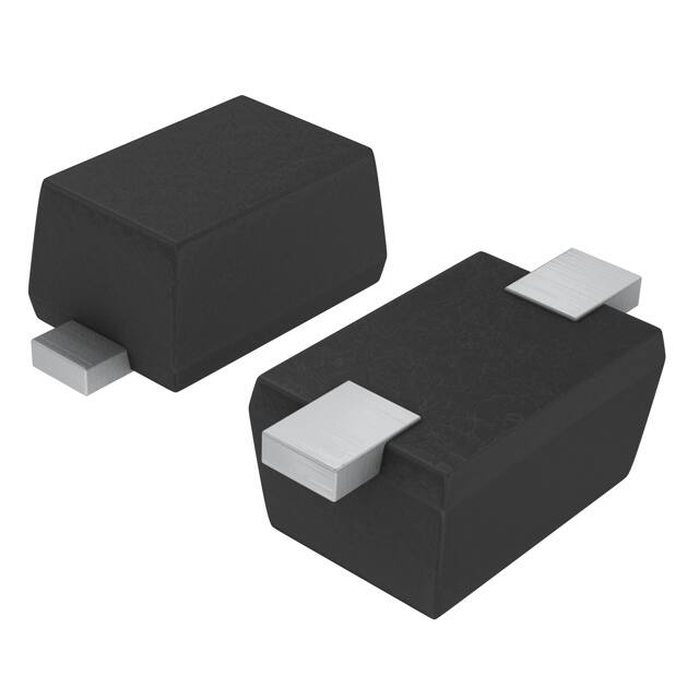
- Package: SOD-123FL
- Essence: Semiconductor material with specific doping to achieve desired voltage characteristics
- Packaging/Quantity: Typically available in reels of 3000 units
Specifications
- Voltage: 10V
- Power Dissipation: 200mW
- Operating Temperature Range: -65°C to +150°C
- Storage Temperature Range: -65°C to +175°C
Detailed Pin Configuration
The EDZTE6110B typically has two pins, with the cathode identified by a band or marking on the body of the diode.
Functional Features
- Precise Voltage Regulation: The EDZTE6110B maintains a constant voltage across its terminals, making it suitable for use in voltage regulation circuits.
- Low Impedance: The diode exhibits low impedance, ensuring minimal impact on the circuit it is integrated into.
- High Reliability: With its stable characteristics and robust construction, the EDZTE6110B offers high reliability in various applications.
Advantages and Disadvantages
Advantages
- Precise voltage regulation
- Low impedance
- High reliability
- Compact package size
Disadvantages
- Limited power dissipation capability
- Sensitivity to temperature variations
Working Principles
The EDZTE6110B operates based on the principle of the Zener effect, where it maintains a nearly constant voltage drop across its terminals when it is reverse-biased and operated within its specified parameters.
Detailed Application Field Plans
The EDZTE6110B finds extensive use in various electronic circuits, including: - Voltage regulators - Overvoltage protection circuits - Signal clamping circuits - Voltage reference circuits
Detailed and Complete Alternative Models
- EDZTE610B: 9V Zener diode with similar characteristics
- EDZTE612B: 11V Zener diode offering a different voltage option
- EDZTE615B: 15V Zener diode with comparable specifications
In conclusion, the EDZTE6110B Zener diode offers precise voltage regulation, low impedance, and high reliability, making it a valuable component in electronic circuits requiring stable voltage references and protection against overvoltage conditions.
Word Count: 386
10 domande e risposte comuni relative all'applicazione di EDZTE6110B nelle soluzioni tecniche
What is EDZTE6110B?
- EDZTE6110B is a high-performance transient voltage suppressor diode designed to protect sensitive electronic equipment from voltage transients induced by lightning, ESD, and other transient voltage events.
What is the maximum clamping voltage of EDZTE6110B?
- The maximum clamping voltage of EDZTE6110B is 14.5V at 10A.
What is the peak pulse power dissipation of EDZTE6110B?
- The peak pulse power dissipation of EDZTE6110B is 600W for an 8/20μs waveform.
What are the typical applications of EDZTE6110B?
- Typical applications of EDZTE6110B include protection of data lines, telecommunications equipment, industrial control systems, and automotive electronics.
What is the operating temperature range of EDZTE6110B?
- The operating temperature range of EDZTE6110B is -55°C to +150°C.
What is the packaging type available for EDZTE6110B?
- EDZTE6110B is available in a variety of surface mount packages including SOD-123FL, SOD-323, and SOD-523.
Is EDZTE6110B RoHS compliant?
- Yes, EDZTE6110B is RoHS compliant, making it suitable for use in environmentally sensitive applications.
What are the key features of EDZTE6110B?
- Key features of EDZTE6110B include low clamping voltage, fast response time, high surge capability, and compatibility with automated placement equipment.
Can EDZTE6110B be used for ESD protection?
- Yes, EDZTE6110B is suitable for ESD protection in various electronic devices and systems.
What are the recommended layout and assembly guidelines for using EDZTE6110B in a circuit?
- The manufacturer provides detailed layout and assembly guidelines in the datasheet to ensure optimal performance and reliability when using EDZTE6110B in a circuit.