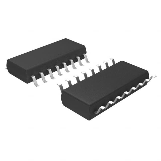
Vedi le specifiche per i dettagli del prodotto.

MM74HC165SJ
Product Overview
- Category: Integrated Circuit
- Use: Shift Register
- Characteristics: Serial-In, Parallel-Out, 8-bit, High-Speed
- Package: SOIC (Small Outline Integrated Circuit)
- Essence: The MM74HC165SJ is a high-speed 8-bit shift register that can be used to expand the number of input/output pins in digital systems.
- Packaging/Quantity: The MM74HC165SJ is available in a tape and reel packaging with a quantity of 2500 units per reel.
Specifications
- Supply Voltage: 2V - 6V
- Operating Temperature Range: -40°C to +85°C
- Input Voltage: 0V - Vcc
- Output Voltage: 0V - Vcc
- Maximum Clock Frequency: 25 MHz
- Number of Input/Output Pins: 16
Detailed Pin Configuration
The MM74HC165SJ has a total of 16 pins. The pin configuration is as follows:
- SER (Serial Data Input)
- QH' (Serial Output)
- QH (Parallel Outputs)
- GND (Ground)
- D7 (Data Input 7)
- D6 (Data Input 6)
- D5 (Data Input 5)
- D4 (Data Input 4)
- D3 (Data Input 3)
- D2 (Data Input 2)
- D1 (Data Input 1)
- D0 (Data Input 0)
- CLK (Clock Input)
- SH/LD (Shift/Load Input)
- MR (Master Reset Input)
- Vcc (Supply Voltage)
Functional Features
- Serial-In, Parallel-Out: The MM74HC165SJ allows data to be serially shifted in and then parallelly outputted.
- High-Speed Operation: With a maximum clock frequency of 25 MHz, the MM74HC165SJ is capable of high-speed data transfer.
- Expandable: Multiple MM74HC165SJ shift registers can be cascaded together to further expand the number of input/output pins.
Advantages and Disadvantages
Advantages
- High-speed operation enables quick data transfer.
- Compact SOIC package saves space on PCBs.
- Expandability allows for flexible system design.
Disadvantages
- Limited number of input/output pins (8-bit).
Working Principles
The MM74HC165SJ operates based on the principle of shifting data through a chain of flip-flops. The serial data input (SER) is shifted into the first flip-flop with each clock pulse. As the clock pulses continue, the data is shifted through the remaining flip-flops until it reaches the last one. At this point, the data is available at the parallel outputs (QH). The shift/load input (SH/LD) controls whether the data is shifted or loaded into the flip-flops. The master reset input (MR) resets all the flip-flops to their initial state.
Detailed Application Field Plans
The MM74HC165SJ can be used in various applications where there is a need to expand the number of input/output pins. Some potential application fields include:
- Microcontroller-based systems
- Data acquisition systems
- Industrial automation
- Robotics
- Communication devices
Detailed and Complete Alternative Models
- SN74HC165N: Similar 8-bit shift register with DIP package
- CD74HC165E: 8-bit shift register with extended temperature range
- 74HCT165: 8-bit shift register with TTL compatibility
(Note: The above alternative models are provided for reference and may have slight differences in specifications and pin configuration.)
Word count: 411 words
10 domande e risposte comuni relative all'applicazione di MM74HC165SJ nelle soluzioni tecniche
Sure! Here are 10 common questions and answers related to the application of MM74HC165SJ in technical solutions:
Q: What is MM74HC165SJ? A: MM74HC165SJ is a 8-bit parallel-in/serial-out shift register IC (Integrated Circuit) that can be used for various digital applications.
Q: What is the purpose of using MM74HC165SJ in technical solutions? A: MM74HC165SJ can be used to expand the number of input pins available on microcontrollers or other digital devices, allowing for the connection of multiple inputs using only a few pins.
Q: How many input pins does MM74HC165SJ have? A: MM74HC165SJ has 8 input pins, which can be used to connect external switches, buttons, sensors, or other digital signals.
Q: How does MM74HC165SJ work? A: MM74HC165SJ works by shifting the state of its input pins into an internal register, which can then be read serially using a clock signal and a data output pin.
Q: Can MM74HC165SJ be used with both 3.3V and 5V systems? A: Yes, MM74HC165SJ is compatible with both 3.3V and 5V systems, making it versatile for various applications.
Q: What is the maximum clock frequency supported by MM74HC165SJ? A: MM74HC165SJ can support clock frequencies up to 25 MHz, allowing for fast data transfer.
Q: Can MM74HC165SJ be cascaded to increase the number of input pins further? A: Yes, multiple MM74HC165SJ ICs can be cascaded together to expand the number of input pins even further.
Q: Does MM74HC165SJ have any built-in debouncing feature for switch inputs? A: No, MM74HC165SJ does not have a built-in debouncing feature. External debouncing circuitry may be required for switch inputs.
Q: Can MM74HC165SJ be used in both digital and analog applications? A: No, MM74HC165SJ is designed for digital applications only and cannot be used directly with analog signals.
Q: Are there any specific precautions to consider when using MM74HC165SJ? A: It is important to ensure that the power supply voltage and clock signal levels are within the specified range (3V to 6V) to avoid damaging the IC. Additionally, proper decoupling capacitors should be used to minimize noise and stabilize the power supply.

