

Vedi le specifiche per i dettagli del prodotto.
MC68HC711D3CFNE3
Product Overview
- Category: Microcontroller
- Use: Control and processing of electronic systems
- Characteristics: High-performance, low-power consumption, versatile
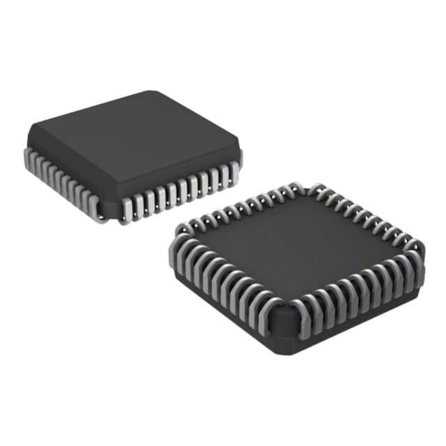
- Package: 52-pin QFP (Quad Flat Package)
- Essence: Integrated circuit for embedded systems
- Packaging/Quantity: Tape and reel packaging, quantity varies
Specifications
- Architecture: 8-bit
- Clock Frequency: Up to 2 MHz
- Program Memory: 4 KB Flash
- RAM: 256 bytes
- I/O Ports: 38
- Timers: 2
- Analog-to-Digital Converter: 8 channels, 8-bit resolution
- Communication Interfaces: SCI (Serial Communication Interface), SPI (Serial Peripheral Interface), I2C (Inter-Integrated Circuit)
Pin Configuration
The MC68HC711D3CFNE3 microcontroller has a total of 52 pins. The pin configuration is as follows:
- VDD - Power supply voltage
- VSS - Ground
- IRQ - Interrupt request input
- PA0 - General-purpose I/O pin
- PA1 - General-purpose I/O pin
- PA2 - General-purpose I/O pin
- PA3 - General-purpose I/O pin
- PA4 - General-purpose I/O pin
- PA5 - General-purpose I/O pin
- PA6 - General-purpose I/O pin
- PA7 - General-purpose I/O pin
- RESET - Reset input
- XTAL - Crystal oscillator input
- EXTAL - Crystal oscillator output
- OSC2 - Oscillator output
- OSC1 - Oscillator input
- PB0 - General-purpose I/O pin
- PB1 - General-purpose I/O pin
- PB2 - General-purpose I/O pin
- PB3 - General-purpose I/O pin
- PB4 - General-purpose I/O pin
- PB5 - General-purpose I/O pin
- PB6 - General-purpose I/O pin
- PB7 - General-purpose I/O pin
- PC0 - General-purpose I/O pin
- PC1 - General-purpose I/O pin
- PC2 - General-purpose I/O pin
- PC3 - General-purpose I/O pin
- PC4 - General-purpose I/O pin
- PC5 - General-purpose I/O pin
- PC6 - General-purpose I/O pin
- PC7 - General-purpose I/O pin
- PD0 - General-purpose I/O pin
- PD1 - General-purpose I/O pin
- PD2 - General-purpose I/O pin
- PD3 - General-purpose I/O pin
- PD4 - General-purpose I/O pin
- PD5 - General-purpose I/O pin
- PD6 - General-purpose I/O pin
- PD7 - General-purpose I/O pin
- PE0 - General-purpose I/O pin
- PE1 - General-purpose I/O pin
- PE2 - General-purpose I/O pin
- PE3 - General-purpose I/O pin
- PE4 - General-purpose I/O pin
- PE5 - General-purpose I/O pin
- PE6 - General-purpose I/O pin
- PE7 - General-purpose I/O pin
- PF0 - General-purpose I/O pin
- PF1 - General-purpose I/O pin
- PF2 - General-purpose I/O pin
- PF3 - General-purpose I/O pin
Functional Features
- High-performance 8-bit microcontroller
- Low-power consumption for energy-efficient applications
- Versatile I/O ports for interfacing with external devices
- Integrated analog-to-digital converter for sensor data acquisition
- Multiple communication interfaces for data exchange
- Built-in timers for precise timing operations
- Flash memory for program storage and easy updates
- Reset input for system initialization
Advantages and Disadvantages
Advantages
- High-performance capabilities suitable for various applications
- Low power consumption extends battery life in portable devices
- Versatile I/O ports allow flexible connectivity options
- Integrated analog-to-digital converter simplifies sensor integration
- Multiple communication interfaces enable seamless data transfer
- Flash memory allows easy program updates without hardware changes
Disadvantages
- Limited program memory (4 KB) may restrict complex applications
- Limited RAM (256 bytes) may limit data processing capabilities
- Clock frequency limited to 2 MHz, which may affect real-time performance in certain applications
Working Principles
The MC68HC711D3CFNE3 microcontroller operates based on the Von Neumann architecture
10 domande e risposte comuni relative all'applicazione di MC68HC711D3CFNE3 nelle soluzioni tecniche
Sure! Here are 10 common questions and answers related to the application of MC68HC711D3CFNE3 in technical solutions:
Q: What is MC68HC711D3CFNE3? A: MC68HC711D3CFNE3 is a microcontroller from the HC11 family, designed for embedded control applications.
Q: What are the key features of MC68HC711D3CFNE3? A: Some key features include an 8-bit CPU, 512 bytes of RAM, 16 KB of ROM, multiple I/O ports, timers, and serial communication interfaces.
Q: What are the typical applications of MC68HC711D3CFNE3? A: MC68HC711D3CFNE3 is commonly used in automotive systems, industrial control systems, consumer electronics, and various other embedded applications.
Q: How can I program MC68HC711D3CFNE3? A: MC68HC711D3CFNE3 can be programmed using assembly language or high-level languages like C, with the help of a suitable development environment and programming tools.
Q: Can MC68HC711D3CFNE3 communicate with other devices? A: Yes, MC68HC711D3CFNE3 supports serial communication protocols like UART (Universal Asynchronous Receiver/Transmitter) and SPI (Serial Peripheral Interface).
Q: What is the maximum clock frequency of MC68HC711D3CFNE3? A: The maximum clock frequency of MC68HC711D3CFNE3 is typically 2 MHz.
Q: Can MC68HC711D3CFNE3 handle interrupts? A: Yes, MC68HC711D3CFNE3 has interrupt capabilities, allowing it to respond to external events and prioritize tasks accordingly.
Q: How many I/O ports are available in MC68HC711D3CFNE3? A: MC68HC711D3CFNE3 has a total of 32 I/O pins, which can be configured as inputs or outputs based on the application requirements.
Q: Is MC68HC711D3CFNE3 suitable for low-power applications? A: Yes, MC68HC711D3CFNE3 is designed to operate at low power levels, making it suitable for battery-powered or energy-efficient devices.
Q: Are there any development tools available for MC68HC711D3CFNE3? A: Yes, there are various development tools, such as compilers, assemblers, debuggers, and emulators, specifically designed for programming and debugging MC68HC711D3CFNE3-based applications.
Please note that the answers provided here are general and may vary depending on specific implementation details and requirements.