

Vedi le specifiche per i dettagli del prodotto.
Encyclopedia Entry: 74LVC374ABQ,115
Product Overview
Category
The 74LVC374ABQ,115 belongs to the category of integrated circuits (ICs) and specifically falls under the family of flip-flops.
Use
This product is commonly used in digital electronics for storing and transferring data. It serves as a latch or register, allowing the storage and retrieval of binary information.
Characteristics
- Low-voltage CMOS technology
- High-speed operation
- Wide operating voltage range
- Schmitt-trigger action on all inputs
- 3-state outputs
- Power-down protection
- Available in various package options
Package
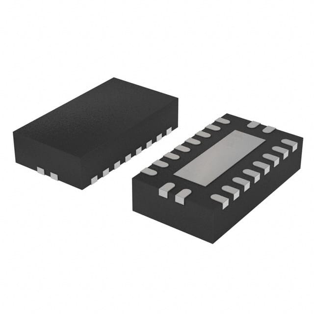
The 74LVC374ABQ,115 is typically available in a small-outline package (SOIC), which provides ease of integration into electronic circuit boards.
Essence
The essence of the 74LVC374ABQ,115 lies in its ability to store and transfer data reliably and efficiently within digital systems.
Packaging/Quantity
This product is usually packaged in reels or tubes, with each reel containing a specific quantity of ICs. The exact quantity may vary depending on the manufacturer's specifications.
Specifications
- Supply Voltage Range: 1.65V to 5.5V
- Input Voltage Range: 0V to VCC
- Output Voltage Range: 0V to VCC
- Operating Temperature Range: -40°C to +125°C
- Maximum Clock Frequency: 100MHz
- Number of Flip-Flops: 8
Detailed Pin Configuration
The 74LVC374ABQ,115 has a total of 20 pins, each serving a specific function. The pin configuration is as follows:
- OE (Output Enable)
- Q0 (Flip-Flop Output 0)
- D0 (Data Input 0)
- D1 (Data Input 1)
- Q1 (Flip-Flop Output 1)
- D2 (Data Input 2)
- D3 (Data Input 3)
- Q2 (Flip-Flop Output 2)
- GND (Ground)
- Q3 (Flip-Flop Output 3)
- D4 (Data Input 4)
- D5 (Data Input 5)
- Q4 (Flip-Flop Output 4)
- D6 (Data Input 6)
- D7 (Data Input 7)
- Q5 (Flip-Flop Output 5)
- VCC (Supply Voltage)
- Q6 (Flip-Flop Output 6)
- Q7 (Flip-Flop Output 7)
- CP (Clock Pulse)
Functional Features
- Data storage and transfer: The 74LVC374ABQ,115 allows for the reliable storage and transfer of binary data within digital systems.
- Schmitt-trigger action: The Schmitt-trigger action on all inputs ensures noise immunity and stable operation in varying input conditions.
- 3-state outputs: The 3-state outputs enable the IC to be connected to multiple devices without causing conflicts or bus contention.
- Power-down protection: This feature protects the IC from potential damage during power-down situations.
Advantages and Disadvantages
Advantages
- High-speed operation enables efficient data processing.
- Wide operating voltage range allows compatibility with various digital systems.
- Schmitt-trigger action ensures reliable operation in noisy environments.
- 3-state outputs facilitate easy integration into complex circuit designs.
- Power-down protection enhances the durability of the IC.
Disadvantages
- Limited number of flip-flops (8) may restrict its use in applications requiring a higher count.
- Availability of alternative models with additional features may limit its competitiveness in certain scenarios.
Working Principles
The 74LVC374ABQ,115 operates based on the principles of flip-flops. It utilizes clock pulses to latch and store data at its inputs, which can then be retrieved from its outputs. The Schmitt-trigger action ensures stable operation by providing hysteresis and noise immunity. The 3-state outputs allow the IC to be connected to multiple devices without causing conflicts or bus contention.
Detailed Application Field Plans
The 74LVC374ABQ,115 finds applications in various digital systems, including but not limited to: - Microcontrollers - Data storage devices - Communication systems - Industrial automation - Consumer electronics
Its ability to store and transfer data reliably makes it suitable for applications where sequential logic and data synchronization are crucial.
Detailed and Complete Alternative Models
While the 74LVC374ABQ,115 offers a range of features and capabilities, alternative models with additional functionalities are available in the market. Some notable alternatives include: - 74HC374: Similar functionality but operates at higher voltages. - 74LS374: Lower power consumption but slower operation speed
10 domande e risposte comuni relative all'applicazione di 74LVC374ABQ,115 nelle soluzioni tecniche
What is the operating voltage range of 74LVC374ABQ,115?
- The operating voltage range of 74LVC374ABQ,115 is 1.65V to 5.5V.What is the maximum output current of 74LVC374ABQ,115?
- The maximum output current of 74LVC374ABQ,115 is ±32mA.Can 74LVC374ABQ,115 be used in automotive applications?
- Yes, 74LVC374ABQ,115 is AEC-Q100 qualified and suitable for automotive applications.What is the typical propagation delay of 74LVC374ABQ,115?
- The typical propagation delay of 74LVC374ABQ,115 is 4.1ns.Is 74LVC374ABQ,115 compatible with 5V TTL/CMOS levels?
- Yes, 74LVC374ABQ,115 is compatible with 5V TTL/CMOS levels.What is the package type of 74LVC374ABQ,115?
- 74LVC374ABQ,115 comes in a standard SO20 package.Can 74LVC374ABQ,115 be used in battery-powered applications?
- Yes, 74LVC374ABQ,115 is suitable for battery-powered applications due to its low power consumption.Does 74LVC374ABQ,115 have overvoltage protection?
- Yes, 74LVC374ABQ,115 has overvoltage input tolerance up to 5.5V.What is the maximum frequency at which 74LVC374ABQ,115 can operate?
- 74LVC374ABQ,115 can operate at a maximum frequency of 200MHz.Is 74LVC374ABQ,115 RoHS compliant?
- Yes, 74LVC374ABQ,115 is RoHS compliant, making it suitable for environmentally friendly designs.