

Vedi le specifiche per i dettagli del prodotto.
Encyclopedia Entry: 74AUP3G0434GMH
Product Information Overview
- Category: Integrated Circuit (IC)
- Use: Logic Gate
- Characteristics: High-speed, low-power consumption
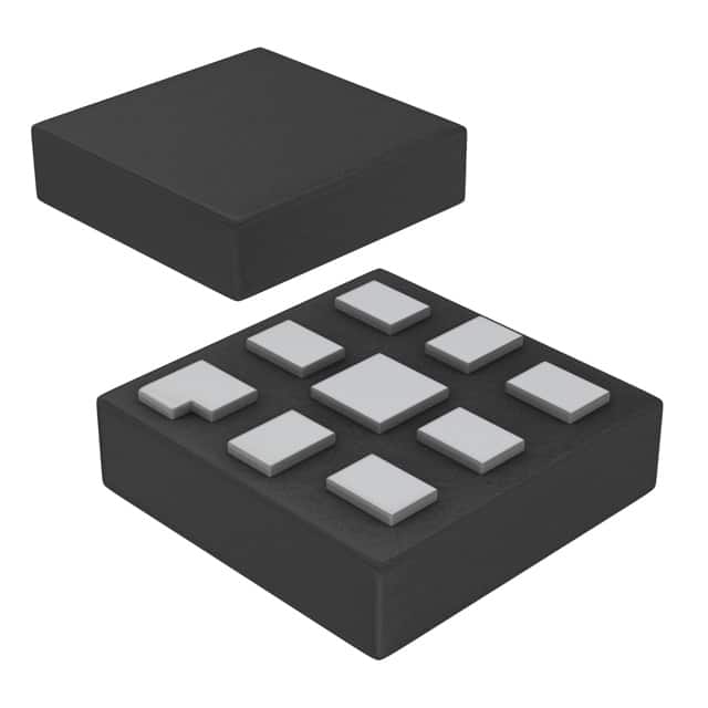
- Package: Miniature Leadless Package (MLP)
- Essence: Triple Buffer/Inverter
- Packaging/Quantity: Available in reels of 3000 units
Specifications
The 74AUP3G0434GMH is a triple buffer/inverter IC designed for high-speed logic applications. It operates at a low power supply voltage and offers excellent noise immunity. The device is compatible with both CMOS and TTL input levels, making it versatile for various digital systems.
Key specifications include:
- Supply Voltage Range: 0.8V to 3.6V
- High-Speed Operation: Propagation Delay of 2.5 ns (typical) at 3.3V
- Low Power Consumption: Maximum Quiescent Current of 1 µA at 3.3V
- Output Drive Capability: ±24 mA at 3.3V
- ESD Protection: Human Body Model > 2000V
Detailed Pin Configuration
The 74AUP3G0434GMH features a compact Miniature Leadless Package (MLP) with six pins. The pin configuration is as follows:
____
   VCC|    |GND
   IN1|    |OUT1
   IN2|    |OUT2
   IN3|    |OUT3
      |____|
Functional Features
The main functional feature of the 74AUP3G0434GMH is its triple buffer/inverter capability. Each input (IN1, IN2, IN3) can be independently buffered or inverted, providing flexibility in signal processing. The outputs (OUT1, OUT2, OUT3) are complementary to the inputs, ensuring efficient logic operations.
Advantages and Disadvantages
Advantages: - High-speed operation enables rapid data processing. - Low power consumption contributes to energy efficiency. - Versatile compatibility with CMOS and TTL input levels. - Compact MLP package allows for space-saving integration. - ESD protection ensures robustness against electrostatic discharge.
Disadvantages: - Limited output drive capability may restrict use in certain applications requiring higher current handling. - Availability in reels of 3000 units may not be suitable for small-scale projects.
Working Principles
The 74AUP3G0434GMH operates based on CMOS technology, utilizing MOSFET transistors to achieve high-speed logic functions. The inputs are buffered or inverted using a combination of transistors, while the outputs are driven by additional transistors to provide the desired logic levels.
Detailed Application Field Plans
The 74AUP3G0434GMH finds applications in various digital systems that require high-speed logic operations with low power consumption. Some potential application fields include:
- Microcontrollers and Microprocessors
- Communication Systems
- Data Storage Devices
- Automotive Electronics
- Industrial Control Systems
Detailed and Complete Alternative Models
For users seeking alternative options, several similar ICs can fulfill comparable functions to the 74AUP3G0434GMH. These include:
- SN74LVC3G34 - Triple Buffer/Inverter IC from Texas Instruments
- MC74VHC1G07 - Single Buffer/Driver IC from ON Semiconductor
- CD74AC14 - Hex Inverter Schmitt Trigger IC from Texas Instruments
- 74HC240 - Octal Buffer/Line Driver IC from NXP Semiconductors
These alternative models offer similar characteristics and can be considered based on specific project requirements.
Word Count: 346 words
10 domande e risposte comuni relative all'applicazione di 74AUP3G0434GMH nelle soluzioni tecniche
Sure! Here are 10 common questions and answers related to the application of 74AUP3G0434GMH in technical solutions:
Q: What is the 74AUP3G0434GMH? A: The 74AUP3G0434GMH is a high-performance, low-power triple buffer with Schmitt-trigger inputs.
Q: What are the key features of the 74AUP3G0434GMH? A: The key features include low power consumption, wide operating voltage range, Schmitt-trigger inputs for noise immunity, and high-speed operation.
Q: What is the typical application of the 74AUP3G0434GMH? A: The 74AUP3G0434GMH is commonly used as a level shifter or signal buffer in various digital systems, such as microcontrollers, FPGAs, and communication interfaces.
Q: What is the operating voltage range of the 74AUP3G0434GMH? A: The 74AUP3G0434GMH can operate within a voltage range of 0.8V to 3.6V.
Q: What is the maximum data rate supported by the 74AUP3G0434GMH? A: The 74AUP3G0434GMH supports a maximum data rate of up to 400 Mbps.
Q: Does the 74AUP3G0434GMH have any built-in ESD protection? A: Yes, the 74AUP3G0434GMH has built-in ESD protection, which helps safeguard against electrostatic discharge events.
Q: Can the 74AUP3G0434GMH be used in both uni-directional and bi-directional applications? A: Yes, the 74AUP3G0434GMH can be used in both uni-directional and bi-directional applications.
Q: What is the power supply voltage required for the 74AUP3G0434GMH? A: The 74AUP3G0434GMH requires a single power supply voltage of 1.2V to 3.6V.
Q: Does the 74AUP3G0434GMH have any specific temperature range limitations? A: The 74AUP3G0434GMH is designed to operate within a temperature range of -40°C to +85°C.
Q: Are there any recommended layout guidelines for using the 74AUP3G0434GMH? A: Yes, it is recommended to follow the manufacturer's layout guidelines, including proper decoupling capacitors placement and minimizing trace lengths for optimal performance.
Please note that these answers are general and may vary depending on the specific application and requirements.