

Vedi le specifiche per i dettagli del prodotto.
SY100E142JC-TR
Product Overview
Category
SY100E142JC-TR belongs to the category of integrated circuits (ICs).
Use
This product is commonly used in electronic devices and systems for signal processing and data transmission.
Characteristics
- High-speed operation
- Low power consumption
- Wide operating voltage range
- Compact size
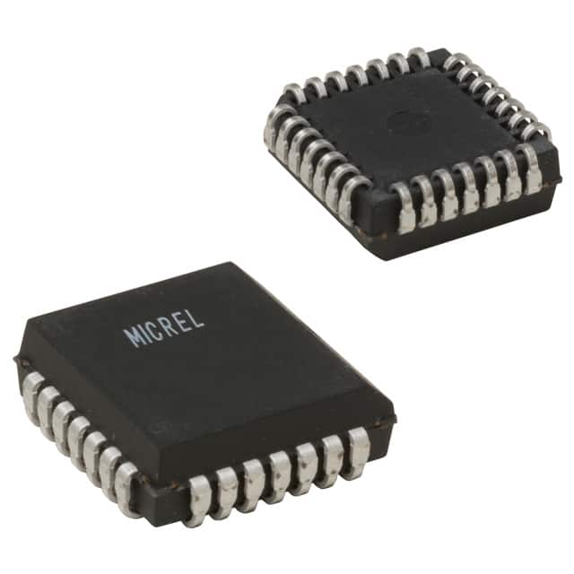
Package
SY100E142JC-TR is available in a small outline package (SOP) with a specified pin configuration.
Essence
The essence of this product lies in its ability to process and transmit signals efficiently and accurately within electronic systems.
Packaging/Quantity
SY100E142JC-TR is typically packaged in reels or tubes, with each containing a specific quantity of ICs.
Specifications
- Operating Voltage Range: 3.0V to 5.5V
- Input Signal Levels: TTL-compatible
- Output Signal Levels: ECL-compatible
- Maximum Clock Frequency: 1.6 GHz
- Number of Pins: 28
- Temperature Range: -40°C to +85°C
Detailed Pin Configuration
The detailed pin configuration of SY100E142JC-TR is as follows:
- VCC
- CLK
- D0
- D1
- D2
- D3
- D4
- D5
- D6
- D7
- D8
- D9
- D10
- D11
- D12
- D13
- D14
- D15
- GND
- Q0
- Q1
- Q2
- Q3
- Q4
- Q5
- Q6
- Q7
- Q8
Functional Features
- High-speed parallel data transmission
- Clock input for synchronous operation
- TTL-compatible inputs and ECL-compatible outputs
- Wide operating voltage range allows compatibility with various systems
Advantages and Disadvantages
Advantages
- High-speed operation enables efficient data processing
- Low power consumption contributes to energy efficiency
- Wide operating voltage range provides flexibility in system integration
- Compact size allows for space-saving designs
Disadvantages
- Limited availability of alternative models
- Higher cost compared to some other ICs with similar functionality
Working Principles
SY100E142JC-TR operates based on the principles of parallel data transmission and clock synchronization. The input signals are processed internally, and the corresponding output signals are generated according to the specified logic.
Detailed Application Field Plans
SY100E142JC-TR finds applications in various fields, including: 1. Telecommunications 2. Data networking 3. Industrial automation 4. Test and measurement equipment 5. High-performance computing
Detailed and Complete Alternative Models
While SY100E142JC-TR is a reliable and widely used IC, there are alternative models available in the market that offer similar functionality. Some notable alternatives include: 1. MC10E141FN 2. CDCLVC1104PW 3. SN74LVCH16245ADGGR
These alternative models can be considered based on specific requirements and compatibility with existing systems.
In conclusion, SY100E142JC-TR is a high-speed integrated circuit used for signal processing and data transmission. Its compact size, low power consumption, and wide operating voltage range make it suitable for various applications. However, limited availability of alternative models and higher cost may be considered as disadvantages.
10 domande e risposte comuni relative all'applicazione di SY100E142JC-TR nelle soluzioni tecniche
Sure! Here are 10 common questions and answers related to the application of SY100E142JC-TR in technical solutions:
Question: What is the purpose of the SY100E142JC-TR?
Answer: The SY100E142JC-TR is a high-speed, low-power ECL-to-TTL translator IC used for converting signals between ECL (Emitter-Coupled Logic) and TTL (Transistor-Transistor Logic) levels.Question: What is the maximum operating frequency of the SY100E142JC-TR?
Answer: The SY100E142JC-TR can operate at frequencies up to 1.5 GHz, making it suitable for high-speed applications.Question: Can the SY100E142JC-TR be used in both input and output signal translation?
Answer: Yes, the SY100E142JC-TR can be used for both translating ECL signals to TTL levels (input translation) and translating TTL signals to ECL levels (output translation).Question: What is the power supply voltage range for the SY100E142JC-TR?
Answer: The SY100E142JC-TR operates with a power supply voltage range of -4.2V to -5.5V for the ECL side and +4.75V to +5.25V for the TTL side.Question: Is the SY100E142JC-TR compatible with other ECL and TTL devices?
Answer: Yes, the SY100E142JC-TR is designed to be compatible with other ECL and TTL devices, allowing for seamless integration into existing systems.Question: What is the typical propagation delay of the SY100E142JC-TR?
Answer: The typical propagation delay of the SY100E142JC-TR is around 1.5 ns, ensuring fast signal translation.Question: Can the SY100E142JC-TR be used in both single-ended and differential signal applications?
Answer: Yes, the SY100E142JC-TR supports both single-ended and differential input/output configurations, providing flexibility in various system designs.Question: Does the SY100E142JC-TR require external components for operation?
Answer: No, the SY100E142JC-TR is a standalone IC and does not require any external components for its basic operation.Question: What is the temperature range for the SY100E142JC-TR?
Answer: The SY100E142JC-TR can operate within a temperature range of -40°C to +85°C, making it suitable for a wide range of environments.Question: Are there any application notes or reference designs available for the SY100E142JC-TR?
Answer: Yes, the manufacturer provides application notes and reference designs that can help users understand and implement the SY100E142JC-TR in their technical solutions effectively.