

Vedi le specifiche per i dettagli del prodotto.
LFXP2-8E-6FTN256I
Product Overview
Category
LFXP2-8E-6FTN256I belongs to the category of Field-Programmable Gate Arrays (FPGAs).
Use
This product is primarily used in digital logic circuits for various applications such as telecommunications, automotive, industrial automation, and consumer electronics.
Characteristics
- High-performance FPGA with advanced features
- Low power consumption
- Flexible and reprogrammable design
- Wide range of I/O interfaces
- High-speed data processing capabilities
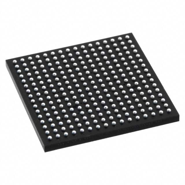
Package
LFXP2-8E-6FTN256I comes in a compact package that ensures easy integration into electronic systems. The package provides protection against environmental factors and facilitates efficient heat dissipation.
Essence
The essence of LFXP2-8E-6FTN256I lies in its ability to provide customizable digital logic functionality, allowing designers to implement complex algorithms and protocols in hardware.
Packaging/Quantity
This product is typically packaged individually and is available in various quantities depending on the customer's requirements.
Specifications
- FPGA Family: LatticeXP2
- Logic Elements: 8,000
- Number of I/Os: 256
- Operating Voltage: 1.2V
- Maximum Frequency: 400 MHz
- Embedded Memory: 576 Kbits
- Package Type: FTBGA
- Temperature Range: -40°C to +100°C
Detailed Pin Configuration
The pin configuration of LFXP2-8E-6FTN256I is as follows:
- Pin 1: VCCIO
- Pin 2: GND
- Pin 3: IO0
- Pin 4: IO1
- ...
- Pin 255: IO254
- Pin 256: IO255
Functional Features
- High-speed data processing: LFXP2-8E-6FTN256I offers fast data processing capabilities, making it suitable for applications that require real-time performance.
- Flexible I/O interfaces: The FPGA supports a wide range of I/O standards, enabling seamless integration with other electronic components.
- Low power consumption: This product is designed to minimize power consumption, making it energy-efficient and suitable for battery-powered devices.
- Reprogrammable design: The FPGA can be reprogrammed multiple times, allowing for iterative development and easy updates.
Advantages and Disadvantages
Advantages
- Customizable logic functionality
- High-performance capabilities
- Wide range of I/O interfaces
- Low power consumption
Disadvantages
- Relatively higher cost compared to fixed-function integrated circuits
- Steeper learning curve for programming and design
Working Principles
LFXP2-8E-6FTN256I operates based on the principles of digital logic. It consists of configurable logic blocks (CLBs), interconnect resources, and I/O elements. The CLBs can be programmed to implement various logic functions, while the interconnect resources facilitate communication between different components within the FPGA. The I/O elements provide interfaces for external connections.
Detailed Application Field Plans
LFXP2-8E-6FTN256I finds applications in various fields, including:
- Telecommunications: Used in network routers, switches, and base stations for high-speed data processing and protocol handling.
- Automotive: Employed in automotive electronics for control systems, driver assistance, and infotainment applications.
- Industrial Automation: Utilized in programmable logic controllers (PLCs) and industrial control systems for process automation and monitoring.
- Consumer Electronics: Integrated into smart TVs, gaming consoles, and multimedia devices for enhanced functionality and performance.
Detailed and Complete Alternative Models
- LFXP2-5E-6FTN256I: Similar to LFXP2-8E-6FTN256I but with 5,000 logic elements.
- LFXP2-12E-6FTN256I: Similar to LFXP2-8E-6FTN256I but with 12,000 logic elements.
- LFXP2-20E-6FTN256I: Similar to LFXP2-8E-6FTN256I but with 20,000 logic elements.
These alternative models provide varying levels of logic capacity to cater to different project requirements.
Word count: 511
10 domande e risposte comuni relative all'applicazione di LFXP2-8E-6FTN256I nelle soluzioni tecniche
Sure! Here are 10 common questions and answers related to the application of LFXP2-8E-6FTN256I in technical solutions:
Q: What is the LFXP2-8E-6FTN256I? A: The LFXP2-8E-6FTN256I is a field-programmable gate array (FPGA) manufactured by Lattice Semiconductor.
Q: What are the key features of the LFXP2-8E-6FTN256I? A: The key features include 8,000 Look-Up Tables (LUTs), 256 I/O pins, low power consumption, and high-speed performance.
Q: What are some typical applications of the LFXP2-8E-6FTN256I? A: The LFXP2-8E-6FTN256I is commonly used in industrial automation, telecommunications, automotive electronics, and consumer electronics.
Q: How can I program the LFXP2-8E-6FTN256I? A: The LFXP2-8E-6FTN256I can be programmed using various development tools such as Lattice Diamond or iCEcube2.
Q: What is the maximum operating frequency of the LFXP2-8E-6FTN256I? A: The maximum operating frequency of the LFXP2-8E-6FTN256I is typically around 300 MHz.
Q: Can I interface the LFXP2-8E-6FTN256I with other components or devices? A: Yes, the LFXP2-8E-6FTN256I supports various interfaces such as SPI, I2C, UART, and GPIOs, allowing easy integration with other components.
Q: What is the power supply voltage range for the LFXP2-8E-6FTN256I? A: The LFXP2-8E-6FTN256I operates on a power supply voltage range of 1.14V to 1.26V.
Q: Can I reprogram the LFXP2-8E-6FTN256I multiple times? A: Yes, the LFXP2-8E-6FTN256I is a reprogrammable FPGA, allowing you to modify the design as needed.
Q: Does the LFXP2-8E-6FTN256I support secure configuration options? A: Yes, the LFXP2-8E-6FTN256I offers security features such as bitstream encryption and authentication to protect your design.
Q: Where can I find additional resources and support for the LFXP2-8E-6FTN256I? A: You can find datasheets, application notes, and technical support on the official website of Lattice Semiconductor or through their authorized distributors.