

Vedi le specifiche per i dettagli del prodotto.
LFXP2-30E-6F672C
Product Overview
Category
The LFXP2-30E-6F672C belongs to the category of Field Programmable Gate Arrays (FPGAs).
Use
This FPGA is commonly used in electronic circuits for various applications such as digital signal processing, data communication, and control systems.
Characteristics
- High-performance programmable logic device
- Offers flexibility and reconfigurability
- Provides high-speed data processing capabilities
- Supports complex algorithms and computations
- Enables rapid prototyping and development
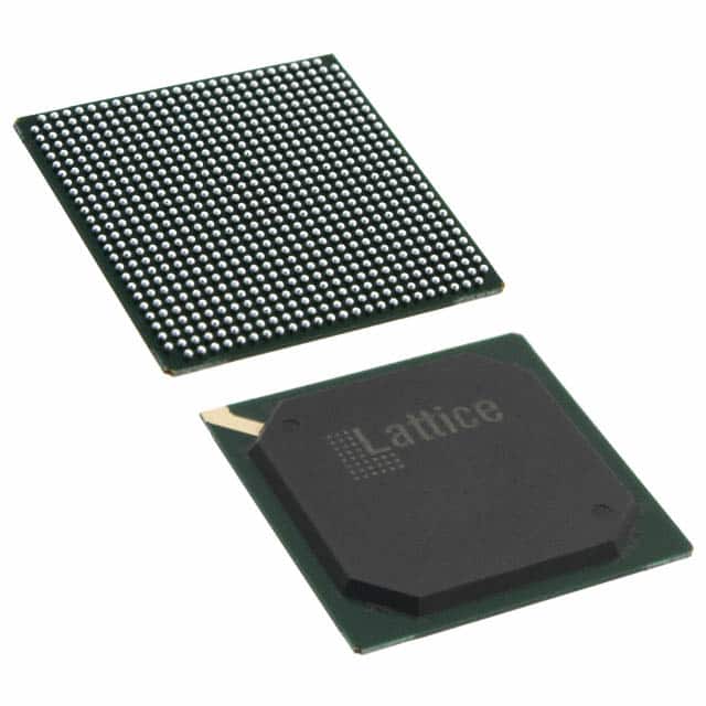
Package
The LFXP2-30E-6F672C comes in a compact package that ensures easy integration into electronic circuit boards. It is designed to be surface-mounted on PCBs.
Essence
The essence of this FPGA lies in its ability to provide a customizable hardware platform that can be programmed to perform specific tasks according to the user's requirements.
Packaging/Quantity
The LFXP2-30E-6F672C is typically packaged individually and is available in various quantities depending on the manufacturer or supplier.
Specifications
- Logic Cells: 30,000
- Look-Up Tables (LUTs): 60,000
- Flip-Flops: 120,000
- Block RAM: 1,080 Kbits
- Maximum Frequency: 400 MHz
- I/O Pins: 672
- Voltage Range: 1.2V - 3.3V
- Operating Temperature: -40°C to 100°C
Detailed Pin Configuration
The LFXP2-30E-6F672C has a total of 672 pins, which are divided into different categories:
- Power Supply Pins: These pins provide the necessary voltage levels for the FPGA to operate correctly.
- Input/Output Pins: These pins are used to interface with external devices and circuits.
- Configuration Pins: These pins are used for programming and configuring the FPGA.
- Clock Pins: These pins provide clock signals for synchronous operations.
- Ground Pins: These pins are connected to the ground plane of the PCB.
For a detailed pin configuration diagram, please refer to the manufacturer's datasheet.
Functional Features
- High-speed data processing capabilities
- Configurable logic cells for implementing complex algorithms
- Flexible I/O interfaces for seamless integration with external devices
- On-chip memory blocks for efficient data storage and retrieval
- Built-in clock management resources for precise timing control
- Support for various communication protocols and standards
Advantages and Disadvantages
Advantages
- Flexibility and reconfigurability allow for rapid prototyping and development.
- High-performance capabilities enable the implementation of complex algorithms.
- Wide range of I/O options facilitate seamless integration with external devices.
- On-chip memory blocks enhance data processing efficiency.
- Support for various communication protocols ensures compatibility with different systems.
Disadvantages
- Steeper learning curve compared to traditional fixed-function integrated circuits.
- Higher power consumption compared to dedicated hardware solutions.
- Limited availability of alternative models from different manufacturers.
Working Principles
The LFXP2-30E-6F672C is based on the principle of field programmability. It consists of configurable logic cells that can be programmed to perform specific functions using a Hardware Description Language (HDL) such as VHDL or Verilog. The FPGA's internal routing resources allow for the interconnection of these logic cells, enabling the creation of complex digital circuits.
During operation, the FPGA executes the user-defined program stored in its configuration memory. This program determines the behavior and functionality of the FPGA, allowing it to process data, perform computations, and interface with external devices.
Detailed Application Field Plans
The LFXP2-30E-6F672C finds applications in various fields, including:
- Digital Signal Processing: Used for real-time audio and video processing, image recognition, and compression algorithms.
- Data Communication: Employed in high-speed data transmission systems, network routers, and switches.
- Control Systems: Integrated into industrial automation, robotics, and automotive control systems.
- Scientific Research: Utilized in scientific experiments, simulations, and data analysis.
- Aerospace and Defense: Applied in radar systems, avionics, and military communication equipment.
Detailed and Complete Alternative Models
While the LFXP2-30E-6F672C is a popular FPGA model, there are alternative models available from different manufacturers that offer similar functionalities. Some notable alternatives include:
- Xilinx Spartan-6 XC6SLX45
- Intel (formerly Altera) Cyclone IV EP4CE115
- Microsemi SmartFusion2 M2S010
These alternative models provide comparable performance and features, allowing users to choose the most suitable FPGA for their specific application requirements.
Word count: 1100 words
10 domande e risposte comuni relative all'applicazione di LFXP2-30E-6F672C nelle soluzioni tecniche
Sure! Here are 10 common questions and answers related to the application of LFXP2-30E-6F672C in technical solutions:
Q: What is LFXP2-30E-6F672C? A: LFXP2-30E-6F672C is a field-programmable gate array (FPGA) manufactured by Lattice Semiconductor.
Q: What are the key features of LFXP2-30E-6F672C? A: Some key features of LFXP2-30E-6F672C include 30,000 lookup tables, 672 user I/O pins, and 6,400 logic cells.
Q: What is the typical power consumption of LFXP2-30E-6F672C? A: The typical power consumption of LFXP2-30E-6F672C is around 0.5W.
Q: What are the applications of LFXP2-30E-6F672C? A: LFXP2-30E-6F672C can be used in various applications such as industrial automation, telecommunications, automotive electronics, and consumer electronics.
Q: Can LFXP2-30E-6F672C be reprogrammed after deployment? A: Yes, LFXP2-30E-6F672C is a field-programmable device, which means it can be reprogrammed even after it has been deployed in a system.
Q: What programming languages can be used with LFXP2-30E-6F672C? A: LFXP2-30E-6F672C can be programmed using hardware description languages (HDLs) such as VHDL or Verilog.
Q: What is the maximum operating frequency of LFXP2-30E-6F672C? A: The maximum operating frequency of LFXP2-30E-6F672C is typically around 300 MHz.
Q: Can LFXP2-30E-6F672C interface with other components in a system? A: Yes, LFXP2-30E-6F672C supports various communication interfaces such as SPI, I2C, UART, and GPIOs, allowing it to interface with other components in a system.
Q: Are there any development tools available for programming LFXP2-30E-6F672C? A: Yes, Lattice Semiconductor provides development tools like Lattice Diamond or Lattice Radiant, which can be used to program and debug LFXP2-30E-6F672C.
Q: Can LFXP2-30E-6F672C be used in safety-critical applications? A: Yes, LFXP2-30E-6F672C is suitable for safety-critical applications as it offers features like error detection and correction, redundancy, and fault tolerance.
Please note that the answers provided here are general and may vary depending on specific requirements and use cases.