

Vedi le specifiche per i dettagli del prodotto.
LFE2-12E-7Q208C
Product Overview
Category
LFE2-12E-7Q208C belongs to the category of Field Programmable Gate Arrays (FPGAs).
Use
This FPGA is commonly used in electronic circuits for digital logic implementation, prototyping, and system integration.
Characteristics
- High flexibility and reconfigurability
- Ability to implement complex digital functions
- Fast processing speed
- Low power consumption
- Compact size
Package
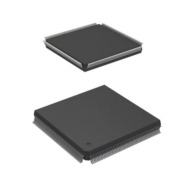
LFE2-12E-7Q208C comes in a Quad Flat No-Lead (QFN) package.
Essence
The essence of LFE2-12E-7Q208C lies in its ability to provide a customizable and versatile solution for digital circuit design and implementation.
Packaging/Quantity
Each package of LFE2-12E-7Q208C contains one FPGA unit.
Specifications
- Model: LFE2-12E-7Q208C
- Logic Elements: 12,000
- Speed Grade: 7
- Package Type: QFN
- Pin Count: 208
- Operating Voltage: 1.2V
- Maximum Frequency: 400 MHz
- I/O Standards: LVCMOS, LVTTL, SSTL, HSTL
Detailed Pin Configuration
The pin configuration of LFE2-12E-7Q208C is as follows:
- Pin 1: VCCIO
- Pin 2: GND
- Pin 3: IOB_0
- Pin 4: IOB_1
- ...
- Pin 207: IOB_204
- Pin 208: IOB_205
Functional Features
- Reconfigurable logic elements for implementing custom digital functions
- Dedicated memory blocks for efficient data storage and retrieval
- Programmable I/O pins for interfacing with external devices
- Clock management resources for precise timing control
- Built-in arithmetic and logic units for mathematical operations
Advantages and Disadvantages
Advantages
- High flexibility allows for rapid prototyping and design iterations
- Lower development costs compared to custom ASICs
- Faster time-to-market due to shorter design cycles
- Ability to reconfigure the FPGA for different applications
- Support for various I/O standards enables easy integration with other components
Disadvantages
- Higher power consumption compared to dedicated hardware solutions
- Limited processing speed compared to specialized processors
- Complexity of programming and configuring the FPGA
- Higher cost per unit compared to mass-produced integrated circuits
Working Principles
LFE2-12E-7Q208C operates based on the principles of configurable logic. It consists of a matrix of programmable logic elements interconnected through configurable routing resources. The user can program the FPGA to implement desired digital functions by configuring the interconnections and functionality of these logic elements.
Detailed Application Field Plans
LFE2-12E-7Q208C finds applications in various fields, including:
- Embedded Systems: Used for implementing control and communication interfaces in embedded systems.
- Digital Signal Processing: Employed for real-time signal processing tasks such as audio and video processing.
- Communications: Utilized in networking equipment for data packet processing and protocol implementation.
- Industrial Automation: Integrated into industrial control systems for process monitoring and control.
- Aerospace and Defense: Used in radar systems, avionics, and military-grade communication systems.
Detailed and Complete Alternative Models
Some alternative models to LFE2-12E-7Q208C are:
- Xilinx Spartan-6 XC6SLX9
- Altera Cyclone IV EP4CE6
- Microsemi ProASIC3 A3P060
- Lattice ECP5-12F
- Intel MAX 10M08
These models offer similar functionality and can be considered as alternatives based on specific project requirements.
In conclusion, LFE2-12E-7Q208C is a versatile FPGA that provides high flexibility, fast processing speed, and low power consumption. It finds applications in various fields such as embedded systems, digital signal processing, communications, industrial automation, and aerospace. While it has advantages in terms of flexibility and time-to-market, it also has disadvantages related to power consumption and complexity. Alternative models are available for consideration based on specific project needs.
10 domande e risposte comuni relative all'applicazione di LFE2-12E-7Q208C nelle soluzioni tecniche
Sure! Here are 10 common questions and answers related to the application of LFE2-12E-7Q208C in technical solutions:
Question: What is the LFE2-12E-7Q208C?
Answer: The LFE2-12E-7Q208C is a specific model of Field-Programmable Gate Array (FPGA) manufactured by Lattice Semiconductor.Question: What are the key features of the LFE2-12E-7Q208C?
Answer: Some key features of this FPGA include 12,000 Look-Up Tables (LUTs), 208-pin Quad Flat No-Lead (QFN) package, and support for various I/O standards.Question: In what applications can the LFE2-12E-7Q208C be used?
Answer: This FPGA can be used in a wide range of applications such as industrial automation, telecommunications, automotive electronics, and consumer electronics.Question: How can I program the LFE2-12E-7Q208C?
Answer: You can program this FPGA using the Lattice Diamond design software or other compatible programming tools provided by Lattice Semiconductor.Question: What is the power supply requirement for the LFE2-12E-7Q208C?
Answer: The recommended power supply voltage for this FPGA is typically 1.2V, but it can operate within a range of 1.14V to 1.26V.Question: Can I interface the LFE2-12E-7Q208C with external devices?
Answer: Yes, this FPGA supports various I/O standards such as LVCMOS, LVTTL, SSTL, and LVDS, allowing you to interface it with a wide range of external devices.Question: What is the maximum operating frequency of the LFE2-12E-7Q208C?
Answer: The maximum operating frequency of this FPGA depends on the specific design and implementation, but it can typically reach frequencies in the range of several hundred megahertz (MHz).Question: Does the LFE2-12E-7Q208C have any built-in security features?
Answer: Yes, this FPGA includes built-in security features such as bitstream encryption and authentication to protect your designs from unauthorized access or tampering.Question: Can I use the LFE2-12E-7Q208C for high-speed data processing?
Answer: Yes, this FPGA is capable of handling high-speed data processing tasks due to its efficient architecture and support for high-performance interfaces.Question: Where can I find more information about the LFE2-12E-7Q208C?
Answer: You can find more detailed information about this FPGA, including datasheets, application notes, and reference designs, on the official website of Lattice Semiconductor or by contacting their technical support team.