

Vedi le specifiche per i dettagli del prodotto.
LC4032ZE-7MN64I
Basic Information Overview
- Category: Integrated Circuit (IC)
- Use: Digital Logic Design and Implementation
- Characteristics:
- Low-power consumption
- High-speed operation
- Small form factor
- Wide operating temperature range
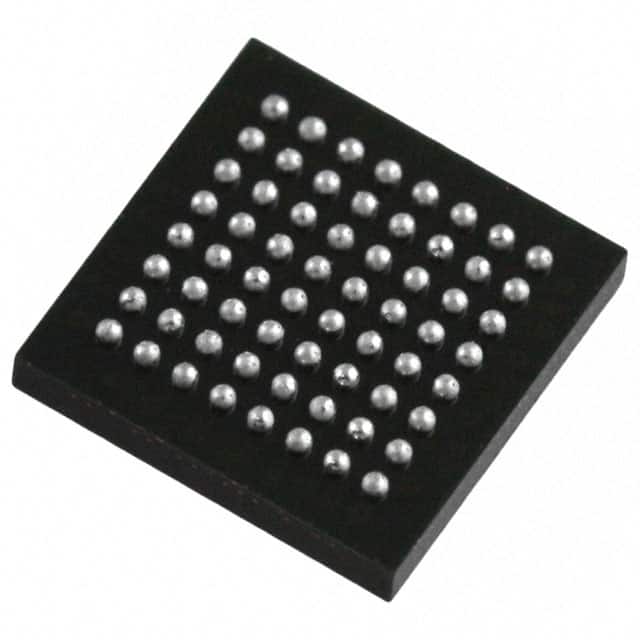
- Package: 64-pin Quad Flat No-Lead (QFN)
- Essence: Programmable Logic Device (PLD)
- Packaging/Quantity: Tray, 250 units per tray
Specifications
- Manufacturer: Lattice Semiconductor Corporation
- Family: ispMACH 4000ZE
- Series: LC4032ZE
- Model: LC4032ZE-7MN64I
- Technology: CMOS Flash-based
- Number of Macrocells: 32
- Operating Voltage: 1.8V to 3.3V
- Operating Frequency: Up to 100 MHz
- I/O Pins: 54
- JTAG Boundary Scan Support: Yes
- User Flash Memory: 32 Kbits
- Speed Grade: 7 (Fastest)
Detailed Pin Configuration
The LC4032ZE-7MN64I has a total of 64 pins, which are assigned for various purposes including power supply, input/output, configuration, and control. The pin configuration is as follows:
- VCCIO: Power supply voltage for I/O pins (1.8V to 3.3V)
- VCCINT: Internal power supply voltage (1.8V to 3.3V)
- GND: Ground reference
- TCK, TDI, TDO, TMS: JTAG boundary scan pins
- IO[0:53]: General-purpose I/O pins
- CONF_DONE: Configuration done output pin
- nCONFIG: Configuration trigger input pin
- nSTATUS: Status output pin indicating device status
- nCE: Chip enable input pin
- nOE: Output enable input pin
- nRW: Read/write control input pin
- nCS: Chip select input pin
Functional Features
- Programmable Logic: The LC4032ZE-7MN64I is a programmable logic device that allows users to implement custom digital logic designs.
- Flash-based Technology: The CMOS flash-based technology enables in-system reconfiguration of the device, allowing for flexibility and ease of design changes.
- Low-power Consumption: The IC is designed to operate with low power consumption, making it suitable for battery-powered applications.
- High-speed Operation: With a maximum operating frequency of 100 MHz, the LC4032ZE-7MN64I can handle high-speed digital signals.
- JTAG Boundary Scan Support: The device supports JTAG boundary scan, facilitating testing and debugging during development.
Advantages and Disadvantages
Advantages: - Flexibility in implementing custom digital logic designs - In-system reconfiguration capability - Low power consumption - High-speed operation - JTAG boundary scan support for easy testing and debugging
Disadvantages: - Limited number of macrocells (32) - Relatively small user flash memory (32 Kbits)
Working Principles
The LC4032ZE-7MN64I operates based on the principles of programmable logic. It consists of configurable logic blocks (CLBs), interconnect resources, I/O buffers, and other supporting components. The CLBs contain look-up tables (LUTs) that can be programmed to implement desired logic functions. The interconnect resources allow for routing signals between different CLBs and I/O pins. By configuring the LUTs and interconnects, users can create complex digital circuits within the device.
Detailed Application Field Plans
The LC4032ZE-7MN64I finds applications in various fields, including: 1. Consumer Electronics: Used in portable devices, gaming consoles, and home appliances for digital logic implementation. 2. Industrial Automation: Employed in control systems, robotics, and process automation for custom logic design and implementation. 3. Automotive Electronics: Integrated into automotive control units, infotainment systems, and driver assistance systems for digital signal processing and control functions. 4. Telecommunications: Utilized in network equipment, routers, and switches for implementing custom logic and protocol handling.
Detailed and Complete Alternative Models
- LC4032ZE-5MN64I: Similar to the LC4032ZE-7MN64I but with a slower speed grade (5).
- LC4032ZE-9MN64I: Similar to the LC4032ZE-7MN64I but with a faster speed grade (9).
- LC4064ZE-7MN64I: A higher-capacity variant with 64 macrocells instead of 32.
These alternative models offer different speed grades or increased capacity while maintaining similar functionality and pin compatibility.
Word count: 526 words
10 domande e risposte comuni relative all'applicazione di LC4032ZE-7MN64I nelle soluzioni tecniche
Sure! Here are 10 common questions and answers related to the application of LC4032ZE-7MN64I in technical solutions:
1. What is LC4032ZE-7MN64I? LC4032ZE-7MN64I is a specific model of Field-Programmable Gate Array (FPGA) manufactured by Lattice Semiconductor Corporation.
2. What are the key features of LC4032ZE-7MN64I? Some key features of LC4032ZE-7MN64I include 32,768 logic cells, 64 I/O pins, low power consumption, and support for various communication protocols.
3. What are the typical applications of LC4032ZE-7MN64I? LC4032ZE-7MN64I is commonly used in applications such as industrial automation, automotive electronics, consumer electronics, telecommunications, and medical devices.
4. How can LC4032ZE-7MN64I be programmed? LC4032ZE-7MN64I can be programmed using Hardware Description Languages (HDLs) like VHDL or Verilog, or through graphical programming tools provided by Lattice Semiconductor.
5. Can LC4032ZE-7MN64I be reprogrammed after deployment? Yes, LC4032ZE-7MN64I is a reprogrammable FPGA, allowing for flexibility in design changes or updates even after deployment.
6. What is the power consumption of LC4032ZE-7MN64I? The power consumption of LC4032ZE-7MN64I depends on the specific design and usage scenario. However, it is known for its low power consumption compared to other FPGAs.
7. Does LC4032ZE-7MN64I support different communication protocols? Yes, LC4032ZE-7MN64I supports various communication protocols such as UART, SPI, I2C, and Ethernet, making it suitable for interfacing with different devices.
8. Can LC4032ZE-7MN64I be used in safety-critical applications? Yes, LC4032ZE-7MN64I can be used in safety-critical applications, provided that the design and implementation meet the necessary safety standards and requirements.
9. What development tools are available for programming LC4032ZE-7MN64I? Lattice Semiconductor provides a range of development tools, including Lattice Diamond, Lattice Radiant, and Lattice Propel, which offer different levels of abstraction for FPGA programming.
10. Are there any limitations or considerations when using LC4032ZE-7MN64I? Some considerations include the limited number of logic cells and I/O pins compared to higher-end FPGAs, as well as the need for proper power management and thermal considerations during system integration.
Please note that these answers are general and may vary depending on specific use cases and requirements.