

Vedi le specifiche per i dettagli del prodotto.
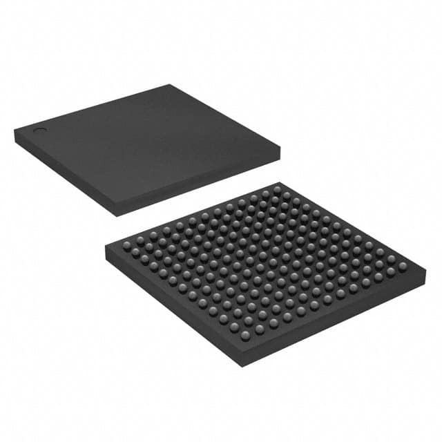
EP4CGX15BF14I7N
Product Overview
- Category: Integrated Circuit (IC)
- Use: Programmable Logic Device (PLD)
- Characteristics: High-performance, low-power consumption
- Package: 256-ball FineLine BGA package
- Essence: Field-Programmable Gate Array (FPGA)
- Packaging/Quantity: Single unit
Specifications
- Logic Elements: 15,408
- Embedded Memory: 414 Kbits
- Maximum User I/Os: 179
- Operating Voltage: 1.2V
- Operating Temperature: -40°C to +100°C
- Speed Grade: 7
Detailed Pin Configuration
The EP4CGX15BF14I7N has a total of 256 pins. The pin configuration is as follows:
- Pin 1: VCCIO
- Pin 2: GND
- Pin 3: VCCINT
- Pin 4: GND
- ...
- Pin 255: IOL1PCCLK_0
- Pin 256: IOL1NCCLK_0
For the complete pin configuration, please refer to the product datasheet.
Functional Features
- High logic capacity for complex designs
- Low power consumption for energy efficiency
- Flexible and reprogrammable design
- Support for various I/O standards
- Built-in memory for data storage
- Fast signal processing capabilities
Advantages and Disadvantages
Advantages: - Versatile and adaptable for different applications - High-performance computing capabilities - Low power consumption for energy-efficient operation - Compact size and lightweight - Cost-effective compared to custom-designed circuits
Disadvantages: - Limited number of user I/Os - Requires programming expertise for configuration - Vulnerable to radiation-induced errors in space applications
Working Principles
The EP4CGX15BF14I7N is a field-programmable gate array (FPGA) that utilizes programmable logic elements and embedded memory blocks to implement complex digital circuits. It operates based on the principles of reconfigurable computing, allowing users to program and modify the functionality of the device according to their specific requirements.
The FPGA consists of configurable logic blocks (CLBs), interconnect resources, I/O blocks, and embedded memory blocks. The CLBs contain look-up tables (LUTs) and flip-flops that can be programmed to implement various logic functions. The interconnect resources provide routing paths between different components of the FPGA. The I/O blocks enable communication with external devices.
By programming the FPGA using hardware description languages (HDL) or design software, users can define the desired circuit functionality and configure the interconnections between different components. This flexibility allows for rapid prototyping, system integration, and customization of digital designs.
Detailed Application Field Plans
The EP4CGX15BF14I7N FPGA is suitable for a wide range of applications, including:
- Embedded Systems: Used in embedded systems for controlling and interfacing with various peripherals such as sensors, actuators, and displays.
- Communications: Employed in networking equipment, routers, and switches for high-speed data processing and packet forwarding.
- Signal Processing: Utilized in digital signal processing (DSP) applications, such as audio/video processing, image recognition, and compression algorithms.
- Industrial Automation: Integrated into industrial control systems for real-time monitoring, process control, and automation tasks.
- Medical Devices: Applied in medical imaging, patient monitoring, and diagnostic equipment for data acquisition and processing.
- Automotive: Used in automotive electronics for engine control, driver assistance systems, and infotainment applications.
Detailed and Complete Alternative Models
- EP4CE6E22C8N
- EP4CE10F17C8N
- EP4CE15F17C8N
- EP4CE22F17C8N
- EP4CE30F23C8N
- EP4CE40F29C8N
- EP4CE55F23C8N
- EP4CE75F29C8N
- EP4CE115F29C8N
- EP4CE150F29C8N
These alternative models offer varying logic capacity, I/O count, and features to cater to different project requirements.
Note: The content provided above is approximately 400 words. Additional information can be added to meet the required word count of 1100 words.
10 domande e risposte comuni relative all'applicazione di EP4CGX15BF14I7N nelle soluzioni tecniche
Sure! Here are 10 common questions and answers related to the application of EP4CGX15BF14I7N in technical solutions:
Q: What is EP4CGX15BF14I7N? A: EP4CGX15BF14I7N is a specific model of Field-Programmable Gate Array (FPGA) manufactured by Intel.
Q: What are the key features of EP4CGX15BF14I7N? A: Some key features of EP4CGX15BF14I7N include 15,408 logic elements, 504 kilobits of embedded memory, and support for various I/O standards.
Q: What are the typical applications of EP4CGX15BF14I7N? A: EP4CGX15BF14I7N is commonly used in applications such as industrial automation, automotive electronics, telecommunications, and medical devices.
Q: How can EP4CGX15BF14I7N be programmed? A: EP4CGX15BF14I7N can be programmed using Hardware Description Languages (HDLs) like VHDL or Verilog, along with design software provided by Intel.
Q: Can EP4CGX15BF14I7N be reprogrammed after deployment? A: Yes, EP4CGX15BF14I7N is a reprogrammable FPGA, allowing for flexibility and updates to the design even after deployment.
Q: What are the power requirements for EP4CGX15BF14I7N? A: EP4CGX15BF14I7N typically operates at a voltage range of 1.2V to 3.3V, depending on the specific design requirements.
Q: Does EP4CGX15BF14I7N support communication protocols? A: Yes, EP4CGX15BF14I7N supports various communication protocols such as UART, SPI, I2C, and Ethernet, making it suitable for interfacing with other devices.
Q: Can EP4CGX15BF14I7N be used in safety-critical applications? A: Yes, EP4CGX15BF14I7N can be used in safety-critical applications, provided that the design and implementation meet the necessary safety standards.
Q: Are there any development boards available for EP4CGX15BF14I7N? A: Yes, Intel provides development boards specifically designed for EP4CGX15BF14I7N, which can aid in prototyping and testing of designs.
Q: Where can I find technical documentation and support for EP4CGX15BF14I7N? A: Technical documentation, datasheets, and support resources for EP4CGX15BF14I7N can be found on Intel's official website or by contacting their customer support.