

Vedi le specifiche per i dettagli del prodotto.
EP3C5E144I7N
Product Overview
- Category: Integrated Circuit (IC)
- Use: Programmable Logic Device (PLD)
- Characteristics: Low-power, high-performance, and highly flexible
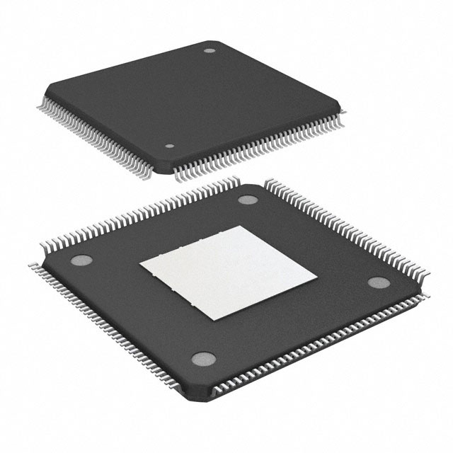
- Package: 144-pin Enhanced Plastic Quad Flat Pack (EPQFP)
- Essence: A versatile PLD with advanced features
- Packaging/Quantity: Available in reels of 250 units
Specifications
- Logic Elements: 5,136
- RAM Bits: 270,336
- Maximum User I/Os: 101
- Clock Management: Phase-Locked Loop (PLL)
- Operating Voltage: 1.2V
- Speed Grade: 7 (Fastest)
Detailed Pin Configuration
The EP3C5E144I7N has a total of 144 pins, each serving a specific purpose. The pin configuration is as follows:
- Pins 1-10: Ground (GND)
- Pins 11-20: VCCIO (I/O Supply Voltage)
- Pins 21-30: Dedicated Input/Output (I/O) Pins
- Pins 31-40: Dedicated Input/Output (I/O) Pins
- Pins 41-50: Dedicated Input/Output (I/O) Pins
- Pins 51-60: Dedicated Input/Output (I/O) Pins
- Pins 61-70: Dedicated Input/Output (I/O) Pins
- Pins 71-80: Dedicated Input/Output (I/O) Pins
- Pins 81-90: Dedicated Input/Output (I/O) Pins
- Pins 91-100: Dedicated Input/Output (I/O) Pins
- Pins 101-110: Dedicated Input/Output (I/O) Pins
- Pins 111-120: Dedicated Input/Output (I/O) Pins
- Pins 121-130: Dedicated Input/Output (I/O) Pins
- Pins 131-140: Dedicated Input/Output (I/O) Pins
- Pins 141-144: Configuration Pins
Functional Features
- High-density programmable logic device with a large number of logic elements
- Flexible I/O configuration for versatile interfacing options
- Efficient clock management using PLL for precise timing control
- Low-power consumption for energy-efficient operation
- Fast speed grade for high-performance applications
- Supports various programming methods for easy configuration
Advantages and Disadvantages
Advantages: - High flexibility and reconfigurability - Large number of logic elements for complex designs - Efficient use of power resources - Fast processing speed for time-critical applications
Disadvantages: - Limited number of user I/Os compared to higher-end models - Relatively small amount of RAM compared to dedicated memory devices - Higher cost compared to simpler PLDs
Working Principles
The EP3C5E144I7N is based on the concept of programmable logic, where the internal circuitry can be configured by the user to perform specific functions. It consists of a matrix of logic elements that can be interconnected to create custom digital circuits. The device is programmed using hardware description languages or design software, which generates a configuration file. This file is then loaded into the PLD, configuring it to perform the desired operations.
Detailed Application Field Plans
The EP3C5E144I7N finds applications in various fields, including:
- Industrial Automation: Used for controlling and monitoring processes in manufacturing plants.
- Communications: Employed in networking equipment for data routing and protocol handling.
- Automotive Electronics: Integrated into automotive systems for control and diagnostics.
- Consumer Electronics: Utilized in devices like gaming consoles and multimedia players for enhanced functionality.
- Medical Devices: Incorporated into medical equipment for data acquisition and signal processing.
Detailed and Complete Alternative Models
- EP3C10E144I7N: Similar to EP3C5E144I7N but with higher logic capacity.
- EP3C16E144I7N: Offers increased logic elements and RAM capacity compared to EP3C5E144I7N.
- EP3C25E144I7N: Provides even greater logic density and I/O capabilities.
- EP3C40E144I7N: Suitable for more complex designs, offering a larger number of logic elements and I/O pins.
- EP3C80E144I7N: High-end model with extensive logic resources and advanced features.
(Note: The above alternative models are just examples and not an exhaustive list.)
Word count: 529 words
10 domande e risposte comuni relative all'applicazione di EP3C5E144I7N nelle soluzioni tecniche
Sure! Here are 10 common questions and answers related to the application of EP3C5E144I7N in technical solutions:
Q: What is EP3C5E144I7N? A: EP3C5E144I7N is a field-programmable gate array (FPGA) chip manufactured by Intel (formerly Altera). It is commonly used in various technical solutions for its programmability and versatility.
Q: What are the key features of EP3C5E144I7N? A: Some key features of EP3C5E144I7N include 5,120 logic elements, 144-pin package, 4 input/output banks, embedded memory blocks, PLLs, and support for various communication protocols.
Q: In what applications can EP3C5E144I7N be used? A: EP3C5E144I7N can be used in a wide range of applications such as industrial automation, robotics, telecommunications, medical devices, automotive systems, and many more.
Q: How does EP3C5E144I7N differ from other FPGA chips? A: EP3C5E144I7N is a specific model of FPGA chip with its own unique specifications. The differences between FPGA chips lie in their capacity, performance, power consumption, and available resources.
Q: Can EP3C5E144I7N be programmed using a specific programming language? A: Yes, EP3C5E144I7N can be programmed using hardware description languages (HDLs) such as VHDL or Verilog. These languages allow designers to describe the desired functionality of the FPGA.
Q: Are there any development tools available for programming EP3C5E144I7N? A: Yes, Intel provides Quartus Prime software suite for designing, simulating, and programming EP3C5E144I7N. It includes a graphical user interface (GUI) and various tools for FPGA development.
Q: Can EP3C5E144I7N be used in real-time applications? A: Yes, EP3C5E144I7N can be used in real-time applications as it offers fast processing capabilities and supports high-speed communication protocols.
Q: Is EP3C5E144I7N suitable for low-power applications? A: EP3C5E144I7N is not specifically designed for low-power applications, but it does offer power-saving features such as clock gating and power optimization techniques that can be utilized to reduce power consumption.
Q: Can EP3C5E144I7N be reprogrammed multiple times? A: Yes, EP3C5E144I7N is a reprogrammable FPGA chip, which means it can be programmed and reprogrammed multiple times to implement different functionalities or fix bugs in the design.
Q: Where can I find more information about EP3C5E144I7N and its applications? A: You can find more detailed information about EP3C5E144I7N, its datasheet, reference designs, and application notes on the official Intel website or by referring to technical documentation and online forums related to FPGA development.