

Vedi le specifiche per i dettagli del prodotto.
5SGXEABK2H40I3L
Product Overview
- Category: Integrated Circuit (IC)
- Use: Digital Logic Device
- Characteristics: High-performance, low-power consumption
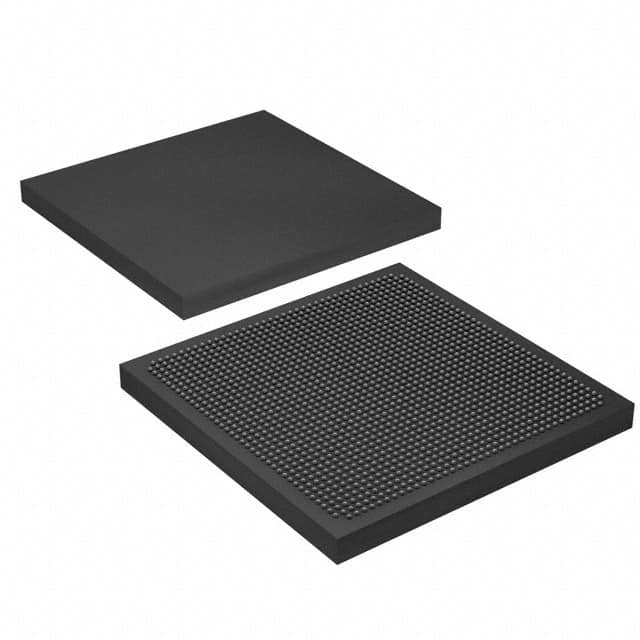
- Package: BGA (Ball Grid Array)
- Essence: Field Programmable Gate Array (FPGA)
- Packaging/Quantity: Single unit
Specifications
- Manufacturer: Intel Corporation
- Technology: 5th Generation Stratix GXE
- Model Number: 5SGXEABK2H40I3L
- Logic Elements: 40,000
- Embedded Memory: 2,048 Kbits
- Operating Voltage: 1.2V
- Operating Temperature: -40°C to +100°C
- Package Dimensions: 35mm x 35mm
- Package Type: Plastic Ball Grid Array (PBGA)
Detailed Pin Configuration
The 5SGXEABK2H40I3L FPGA has a total of 484 pins, which are distributed across various functional groups. The pin configuration includes power supply pins, ground pins, input/output pins, clock pins, and configuration pins. Each pin serves a specific purpose and is labeled accordingly.
Functional Features
- High-speed performance: The 5SGXEABK2H40I3L FPGA offers fast processing capabilities, making it suitable for applications requiring real-time data processing.
- Low-power consumption: This FPGA is designed to minimize power consumption, enabling energy-efficient operation in various electronic systems.
- Flexibility: Being a field-programmable device, the 5SGXEABK2H40I3L allows users to reconfigure its internal logic according to their specific requirements.
- Scalability: With 40,000 logic elements, this FPGA provides ample resources for implementing complex digital designs.
- Robust design: The 5SGXEABK2H40I3L is built to withstand harsh operating conditions, ensuring reliable performance in demanding environments.
Advantages and Disadvantages
Advantages
- Versatility: The FPGA's programmable nature allows it to be used in a wide range of applications, from telecommunications to industrial automation.
- Customizability: Users can tailor the FPGA's functionality to suit their specific needs, eliminating the need for custom-designed ASICs.
- Time-to-market: FPGA-based solutions can be developed and deployed faster compared to traditional hardware designs.
- Cost-effective: FPGAs offer cost advantages over ASICs for low to medium volume production runs.
Disadvantages
- Complexity: Designing and programming an FPGA requires specialized knowledge and expertise.
- Limited performance optimization: While FPGAs provide high flexibility, they may not achieve the same level of performance as dedicated ASICs for certain applications.
- Higher power consumption: Compared to application-specific integrated circuits (ASICs), FPGAs typically consume more power due to their reconfigurable nature.
Working Principles
The 5SGXEABK2H40I3L FPGA operates based on the principles of configurable logic. It consists of an array of programmable logic elements interconnected through configurable routing resources. These logic elements can be programmed to implement various digital functions, such as arithmetic operations, memory storage, and control logic. The configuration of the FPGA is stored in non-volatile memory and can be modified by the user as needed.
Detailed Application Field Plans
The 5SGXEABK2H40I3L FPGA finds applications in diverse fields, including:
- Telecommunications: Used in base stations, routers, and network switches for high-speed data processing and protocol handling.
- Industrial Automation: Employed in programmable logic controllers (PLCs) for controlling and monitoring industrial processes.
- Automotive: Integrated into automotive electronics for functions like advanced driver assistance systems (ADAS) and infotainment systems.
- Aerospace and Defense: Utilized in radar systems, avionics, and military communication equipment for their high-performance computing capabilities.
Detailed and Complete Alternative Models
- 5SGXEABK2H40C2N: Similar to the 5SGXEABK2H40I3L, but with different package dimensions.
- 5SGXEABK2H40E2L: Offers enhanced features and increased logic capacity compared to the 5SGXEABK2H40I3L.
- 5SGXEABK2H40M2N: Designed for applications requiring extended temperature range and ruggedness.
These alternative models provide options with varying specifications and features to cater to different project requirements.
Note: The content provided above is a sample structure for an encyclopedia entry and may not reflect actual product details.
10 domande e risposte comuni relative all'applicazione di 5SGXEABK2H40I3L nelle soluzioni tecniche
Sure! Here are 10 common questions and answers related to the application of 5SGXEABK2H40I3L in technical solutions:
Q: What is the purpose of the 5SGXEABK2H40I3L FPGA? A: The 5SGXEABK2H40I3L is a Field-Programmable Gate Array (FPGA) designed for implementing complex digital logic circuits in various technical solutions.
Q: What are some typical applications of the 5SGXEABK2H40I3L FPGA? A: The 5SGXEABK2H40I3L FPGA can be used in applications such as high-performance computing, telecommunications, industrial automation, image processing, and data center acceleration.
Q: How does the 5SGXEABK2H40I3L FPGA differ from other FPGAs? A: The 5SGXEABK2H40I3L FPGA offers a specific combination of features, performance, and capacity that makes it suitable for demanding applications requiring high-speed processing and large-scale integration.
Q: Can the 5SGXEABK2H40I3L FPGA be reprogrammed after deployment? A: Yes, FPGAs like the 5SGXEABK2H40I3L can be reprogrammed multiple times, allowing for flexibility and adaptability in the field.
Q: What tools are available for programming the 5SGXEABK2H40I3L FPGA? A: Intel Quartus Prime is the primary software tool used for designing, programming, and debugging the 5SGXEABK2H40I3L FPGA.
Q: What interfaces does the 5SGXEABK2H40I3L FPGA support? A: The 5SGXEABK2H40I3L FPGA supports various interfaces such as PCIe, Ethernet, USB, DDR memory, and high-speed serial transceivers.
Q: Can the 5SGXEABK2H40I3L FPGA be used in safety-critical applications? A: Yes, the 5SGXEABK2H40I3L FPGA can be used in safety-critical applications, but additional design considerations and validation processes may be required to meet specific safety standards.
Q: What is the power consumption of the 5SGXEABK2H40I3L FPGA? A: The power consumption of the 5SGXEABK2H40I3L FPGA depends on the specific configuration and utilization, but it is generally designed to be power-efficient.
Q: Are there any known limitations or constraints when using the 5SGXEABK2H40I3L FPGA? A: Like any electronic component, the 5SGXEABK2H40I3L FPGA has certain limitations and constraints, such as maximum operating frequency, available I/O pins, and resource utilization. These should be considered during the design phase.
Q: Where can I find more information about the 5SGXEABK2H40I3L FPGA? A: You can refer to the official documentation provided by the FPGA manufacturer, Intel (formerly Altera), for detailed specifications, application notes, reference designs, and user guides related to the 5SGXEABK2H40I3L FPGA.
Please note that the specific details and answers may vary depending on the context and requirements of your technical solution.