

Vedi le specifiche per i dettagli del prodotto.
Encyclopedia Entry: 74FCT543ATQG
Product Overview
Category
The 74FCT543ATQG belongs to the category of integrated circuits (ICs) and specifically falls under the group of octal transparent latches with 3-state outputs.
Use
This product is commonly used in digital systems for data storage and transfer. It serves as a latch, allowing the temporary storage of data before it is transferred to other components or processed further.
Characteristics
- Octal transparent latch: The 74FCT543ATQG consists of eight individual transparent latches, each capable of storing one bit of data.
- 3-state outputs: The outputs of this IC can be put into a high-impedance state, allowing multiple devices to share a common bus without interfering with each other.
- High-speed operation: The 74FCT543ATQG is designed for fast data transfer, making it suitable for applications that require quick response times.
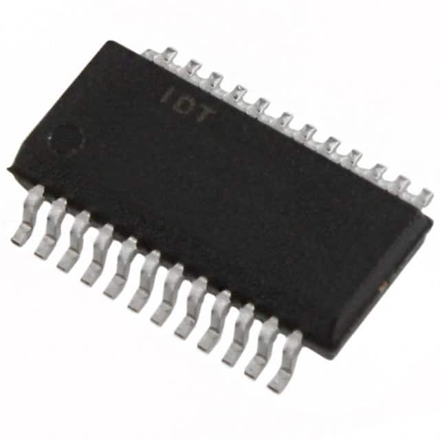
Package and Quantity
This IC is available in a standard 20-pin TSSOP (Thin Shrink Small Outline Package) package. It is typically sold in reels containing a quantity of 250 units.
Specifications
- Supply Voltage Range: 4.5V to 5.5V
- Input Voltage Range: 0V to Vcc
- Output Voltage Range: 0V to Vcc
- Operating Temperature Range: -40°C to +85°C
- Maximum Clock Frequency: 100MHz
Pin Configuration
The 74FCT543ATQG has a total of 20 pins, which are assigned specific functions as follows:
- GND: Ground
- D0: Data input/output 0
- D1: Data input/output 1
- D2: Data input/output 2
- D3: Data input/output 3
- D4: Data input/output 4
- D5: Data input/output 5
- D6: Data input/output 6
- D7: Data input/output 7
- OE: Output Enable
- LE: Latch Enable
- CLK: Clock Input
- GND: Ground
- Q0: Output 0
- Q1: Output 1
- Q2: Output 2
- Q3: Output 3
- Q4: Output 4
- Q5: Output 5
- Q6: Output 6
Functional Features
- Transparent latch operation: The 74FCT543ATQG allows data to pass through when the latch enable (LE) input is high, providing a transparent path for data transfer.
- 3-state outputs: The output enable (OE) input controls the state of the outputs. When OE is low, the outputs are active and reflect the stored data. When OE is high, the outputs enter a high-impedance state.
- Edge-triggered clocking: The IC utilizes a clock input (CLK) to latch the data into its internal storage elements. The data is captured on the rising edge of the clock signal.
Advantages and Disadvantages
Advantages
- High-speed operation enables efficient data transfer in time-critical applications.
- 3-state outputs allow for bus sharing and reduce the need for additional components.
- Octal configuration provides flexibility in handling multiple data inputs/outputs.
Disadvantages
- Limited voltage range may restrict compatibility with certain systems.
- TSSOP package may require careful handling during assembly due to its small size.
Working Principles
The 74FCT543ATQG operates based on the principle of transparent latching. When the latch enable (LE) input is high, the data inputs (D0-D7) are directly connected to the outputs (Q0-Q6). This allows the data to pass through the IC without any delay.
The clock input (CLK) triggers the latching action. On the rising edge of the clock signal, the data present at the inputs is captured and stored in the internal storage elements. The stored data remains unchanged until the next rising edge of the clock.
The output enable (OE) input controls the state of the outputs. When OE is low, the stored data is available at the outputs. Conversely, when OE is high, the outputs enter a high-impedance state, effectively disconnecting them from the external circuitry.
Application Field Plans
The 74FCT543ATQG finds applications in various digital systems where data storage and transfer are essential. Some potential application fields include:
- Microprocessors: Used for temporary storage of data during processing.
- Communication Systems: Facilitates data transfer between different components.
- Memory Modules: Enables efficient data handling within memory units.
10 domande e risposte comuni relative all'applicazione di 74FCT543ATQG nelle soluzioni tecniche
Sure! Here are 10 common questions and answers related to the application of 74FCT543ATQG in technical solutions:
Question: What is the function of the 74FCT543ATQG?
Answer: The 74FCT543ATQG is an octal transparent latch with 3-state outputs.Question: What is the maximum operating voltage for this IC?
Answer: The maximum operating voltage for the 74FCT543ATQG is 5.5V.Question: How many latch inputs does this IC have?
Answer: The 74FCT543ATQG has 8 latch inputs, one for each latch.Question: Can I use this IC in a 3.3V system?
Answer: Yes, the 74FCT543ATQG is compatible with both 5V and 3.3V systems.Question: What is the output current capability of this IC?
Answer: The 74FCT543ATQG has a typical output current capability of ±12mA.Question: Does this IC have internal pull-up or pull-down resistors?
Answer: No, the 74FCT543ATQG does not have internal pull-up or pull-down resistors.Question: Can I connect multiple 74FCT543ATQG ICs together?
Answer: Yes, you can connect multiple 74FCT543ATQG ICs together to expand the number of latches.Question: What is the propagation delay of this IC?
Answer: The propagation delay of the 74FCT543ATQG is typically 5ns.Question: Can I use this IC in high-speed applications?
Answer: Yes, the 74FCT543ATQG is designed for high-speed operation.Question: Does this IC have any built-in protection features?
Answer: Yes, the 74FCT543ATQG has built-in ESD protection on all inputs and outputs.
Please note that these answers are general and may vary depending on the specific datasheet and manufacturer's specifications of the 74FCT543ATQG.