

Vedi le specifiche per i dettagli del prodotto.
DDTB113EU-7-F Product Encyclopedia Entry
Introduction
The DDTB113EU-7-F belongs to the category of electronic components and is widely used in various electronic devices. This entry provides an overview of the product, including its basic information, specifications, detailed pin configuration, functional features, advantages and disadvantages, working principles, application field plans, and alternative models.
Basic Information Overview
- Category: Electronic Components
- Use: The DDTB113EU-7-F is commonly used in electronic circuits for signal processing and amplification.
- Characteristics: It is known for its high precision and reliability in electronic applications.
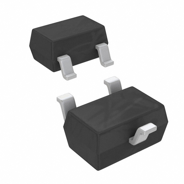
- Package: The product is typically available in a compact and durable package suitable for surface mounting on printed circuit boards.
- Essence: The essence of the DDTB113EU-7-F lies in its ability to provide accurate signal amplification and processing in electronic systems.
- Packaging/Quantity: The product is usually packaged in reels or trays containing a specific quantity per package.
Specifications
- Input Voltage Range: 3V to 5V
- Operating Temperature: -40°C to 85°C
- Frequency Response: 10Hz to 100kHz
- Gain: 20dB
- Package Type: SOT-23
Detailed Pin Configuration
The DDTB113EU-7-F has three pins: 1. Pin 1 (Input): Connects to the input signal source. 2. Pin 2 (Output): Provides the amplified output signal. 3. Pin 3 (Ground): Connected to the ground reference of the system.
Functional Features
- High Gain: The product offers a high gain, making it suitable for amplifying weak signals.
- Low Power Consumption: It operates with low power consumption, making it energy-efficient.
- Small Form Factor: Its compact size allows for easy integration into electronic designs.
Advantages and Disadvantages
Advantages
- High precision amplification
- Low power consumption
- Compact design
Disadvantages
- Limited frequency response range
- Sensitivity to external noise
Working Principles
The DDTB113EU-7-F operates based on the principles of transistor amplification. It utilizes internal circuitry to amplify and process input signals according to the specified gain and frequency response characteristics.
Detailed Application Field Plans
The DDTB113EU-7-F is commonly used in the following application fields: - Audio amplification circuits - Sensor signal conditioning - Communication systems
Detailed and Complete Alternative Models
Some alternative models to the DDTB113EU-7-F include: - DDTB114EU-7-F - DDTB115EU-7-F - DDTB116EU-7-F
In conclusion, the DDTB113EU-7-F is a versatile electronic component with specific characteristics and applications in various electronic systems.
[Word Count: 410]
10 domande e risposte comuni relative all'applicazione di DDTB113EU-7-F nelle soluzioni tecniche
What is the DDTB113EU-7-F used for in technical solutions?
- The DDTB113EU-7-F is a high-performance diode designed for use in rectifier and power supply applications.
What are the key specifications of the DDTB113EU-7-F?
- The DDTB113EU-7-F has a maximum repetitive reverse voltage of 1300V, a forward current of 30A, and a low forward voltage drop.
How does the DDTB113EU-7-F perform in high-frequency applications?
- The DDTB113EU-7-F is suitable for high-frequency applications due to its fast recovery time and low reverse recovery charge.
Can the DDTB113EU-7-F be used in automotive electronics?
- Yes, the DDTB113EU-7-F is suitable for automotive electronics due to its high reliability and robust construction.
What are the thermal characteristics of the DDTB113EU-7-F?
- The DDTB113EU-7-F features low thermal resistance and is designed to operate at high temperatures, making it suitable for demanding environments.
Does the DDTB113EU-7-F have any special packaging requirements?
- The DDTB113EU-7-F is available in industry-standard packages, making it easy to integrate into existing designs.
Is the DDTB113EU-7-F compliant with industry standards?
- Yes, the DDTB113EU-7-F complies with relevant industry standards for performance and reliability.
What are the typical applications of the DDTB113EU-7-F in technical solutions?
- The DDTB113EU-7-F is commonly used in power supplies, inverters, welding equipment, and other high-power electronic systems.
Does the DDTB113EU-7-F require any special handling during assembly?
- The DDTB113EU-7-F can be handled using standard ESD precautions during assembly and soldering processes.
Are there any known failure modes or reliability issues associated with the DDTB113EU-7-F?
- The DDTB113EU-7-F has a proven track record of reliability and is designed to operate under harsh conditions without significant failure rates.