

Vedi le specifiche per i dettagli del prodotto.
S29AL016J55BFNR10
Basic Information Overview
- Category: Flash Memory
- Use: Data storage and retrieval in electronic devices
- Characteristics:
- Non-volatile memory
- High-speed read and write operations
- Low power consumption
- Large storage capacity
- Package: BGA (Ball Grid Array)
- Essence: Reliable and efficient data storage solution
- Packaging/Quantity: Available in reels, quantity varies based on customer requirements
Specifications
- Manufacturer: Cypress Semiconductor
- Memory Type: NOR Flash
- Density: 16 Megabits (2 Megabytes)
- Organization: 2 M x 8 bits
- Voltage Range: 2.7V - 3.6V
- Operating Temperature Range: -40°C to +85°C
- Speed: 55 ns (Read), 55 ns (Program), 55 ns (Erase)
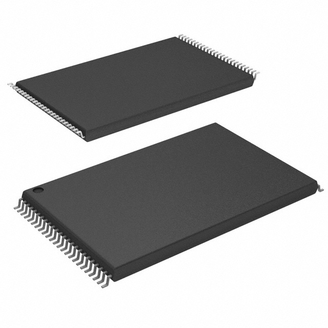
Detailed Pin Configuration
The S29AL016J55BFNR10 has a total of 48 pins. The pin configuration is as follows:
- VCC
- A0
- A1
- A2
- A3
- A4
- A5
- A6
- A7
- A8
- A9
- A10
- A11
- A12
- A13
- A14
- A15
- A16
- A17
- A18
- A19
- A20
- A21
- A22
- A23
- BYTE#
- WE#
- CE#
- OE#
- RY/BY#
- DQ0
- DQ1
- DQ2
- DQ3
- DQ4
- DQ5
- DQ6
- DQ7
- VSS
- NC
- NC
- NC
- NC
- NC
- NC
- NC
- NC
- NC
Functional Features
- High-speed read and write operations enable fast data access.
- Non-volatile memory retains data even when power is disconnected.
- Low power consumption makes it suitable for battery-powered devices.
- Large storage capacity allows for storing a significant amount of data.
Advantages
- Reliable and durable data storage solution.
- Fast read and write operations enhance overall system performance.
- Low power consumption prolongs battery life in portable devices.
- Wide operating temperature range enables usage in various environments.
Disadvantages
- Limited storage capacity compared to higher-density flash memory options.
- Higher cost per megabyte compared to some other memory technologies.
- BGA package may require specialized equipment for installation or replacement.
Working Principles
The S29AL016J55BFNR10 utilizes NOR flash memory technology. It stores data by trapping electrons in a floating gate, which can be electrically programmed and erased. When reading data, the stored charge is detected, allowing retrieval of the information. The device operates based on a combination of address lines, control signals, and data lines to perform read, write, and erase operations.
Detailed Application Field Plans
The S29AL016J55BFNR10 is widely used in various electronic devices that require non-volatile data storage. Some common application fields include: - Consumer electronics (e.g., smartphones, tablets, digital cameras) - Automotive systems (e.g., infotainment systems, instrument clusters) - Industrial equipment (e.g., control systems, data loggers) - Medical devices (e.g., patient monitoring systems, diagnostic equipment)
Detailed and Complete Alternative Models
- S29AL016D70TFI020: Same density, faster speed (70 ns)
- S29GL032N90TFI040: Higher density (32 Megabits), faster speed (90 ns)
- S29GL064N90TFI070: Higher density (64 Megabits), faster speed (90 ns)
- S29GL128N90TFI010: Higher density (128 Megabits), faster speed (90 ns)
(Note: The above alternative models are provided as examples and may not cover all available options.)
This entry provides a comprehensive overview of the S29AL016J55BFNR10 flash memory. It includes basic information, specifications, pin configuration, functional features, advantages and disadvantages, working principles, application field plans, and alternative models.
10 domande e risposte comuni relative all'applicazione di S29AL016J55BFNR10 nelle soluzioni tecniche
Sure! Here are 10 common questions and answers related to the application of S29AL016J55BFNR10 in technical solutions:
Q: What is the S29AL016J55BFNR10? A: The S29AL016J55BFNR10 is a specific model of flash memory chip manufactured by Cypress Semiconductor.
Q: What is the storage capacity of the S29AL016J55BFNR10? A: The S29AL016J55BFNR10 has a storage capacity of 16 megabits (2 megabytes).
Q: What is the operating voltage range for this chip? A: The S29AL016J55BFNR10 operates within a voltage range of 2.7V to 3.6V.
Q: What is the maximum data transfer rate supported by this chip? A: The S29AL016J55BFNR10 supports a maximum data transfer rate of 55 MHz.
Q: Can this chip be used in industrial applications? A: Yes, the S29AL016J55BFNR10 is suitable for use in various industrial applications due to its reliability and durability.
Q: Does this chip support hardware or software write protection? A: Yes, the S29AL016J55BFNR10 supports both hardware and software write protection mechanisms.
Q: Is this chip compatible with standard microcontrollers? A: Yes, the S29AL016J55BFNR10 is designed to be compatible with a wide range of microcontrollers.
Q: What is the typical lifespan of this flash memory chip? A: The S29AL016J55BFNR10 has a typical lifespan of 100,000 program/erase cycles.
Q: Can this chip operate in extreme temperature conditions? A: Yes, the S29AL016J55BFNR10 is designed to operate within a wide temperature range, typically from -40°C to +85°C.
Q: Are there any specific programming requirements for this chip? A: Yes, the S29AL016J55BFNR10 requires specific programming algorithms and voltage levels for proper operation. Please refer to the datasheet for detailed instructions.
Please note that these answers are general and may vary depending on the specific application and requirements. It's always recommended to consult the datasheet or contact the manufacturer for accurate and up-to-date information.