

Vedi le specifiche per i dettagli del prodotto.
CDBD640-G Product Overview
Introduction
The CDBD640-G is a versatile electronic component that belongs to the category of semiconductor devices. This product is widely used in various electronic applications due to its unique characteristics and functional features.
Basic Information Overview
- Category: Semiconductor Device
- Use: Electronic Applications
- Characteristics: Versatile, Reliable, High Performance
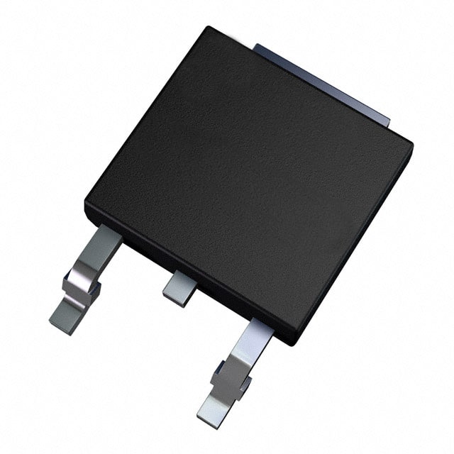
- Package: TO-220AB
- Essence: Power Rectifier
- Packaging/Quantity: 50 pieces per pack
Specifications
The detailed specifications of the CDBD640-G are as follows: - Maximum Average Forward Current: 6A - Maximum Peak Reverse Voltage: 400V - Operating Temperature Range: -65°C to +175°C - Forward Voltage Drop: 1.1V at 3A - Reverse Recovery Time: 35ns
Detailed Pin Configuration
The CDBD640-G has a standard TO-220AB package with three pins: 1. Pin 1: Anode 2. Pin 2: Cathode 3. Pin 3: Not connected (Tab)
Functional Features
- High forward current capability
- Fast reverse recovery time
- Low forward voltage drop
- Excellent thermal performance
Advantages and Disadvantages
Advantages
- Reliable and durable
- Suitable for high-power applications
- Fast switching speed
Disadvantages
- Higher forward voltage drop compared to some alternative models
- Sensitive to temperature variations
Working Principles
The CDBD640-G operates based on the principles of rectification and fast recovery. When a forward voltage is applied, it allows current to flow in one direction while blocking it in the reverse direction. The fast recovery time ensures minimal energy loss during switching operations.
Detailed Application Field Plans
The CDBD640-G is commonly used in the following application fields: - Power supplies - Motor drives - Inverters - Welding equipment - Battery chargers
Detailed and Complete Alternative Models
Some alternative models to the CDBD640-G include: - CDBD650-G - CDBD630-G - CDBD620-G
In summary, the CDBD640-G is a reliable semiconductor device with versatile applications in various electronic systems. Its high-performance characteristics make it a preferred choice for power rectification and fast switching operations.
[Word Count: 340]
10 domande e risposte comuni relative all'applicazione di CDBD640-G nelle soluzioni tecniche
What is CDBD640-G?
- CDBD640-G is a high-performance digital signal processor (DSP) designed for use in technical solutions requiring advanced signal processing capabilities.
What are the key features of CDBD640-G?
- The key features of CDBD640-G include high-speed processing, multiple I/O interfaces, low power consumption, and support for various signal processing algorithms.
How can CDBD640-G be integrated into a technical solution?
- CDBD640-G can be integrated into a technical solution by connecting it to sensors, actuators, and other components through its I/O interfaces, and programming it to perform specific signal processing tasks.
What types of applications is CDBD640-G suitable for?
- CDBD640-G is suitable for applications such as audio processing, image processing, control systems, communication systems, and industrial automation.
Does CDBD640-G support real-time processing?
- Yes, CDBD640-G supports real-time processing, making it suitable for applications that require low latency and high-speed data processing.
What programming languages can be used to develop applications for CDBD640-G?
- CDBD640-G can be programmed using languages such as C/C++ and assembly language, with support for development tools and libraries provided by the manufacturer.
Can CDBD640-G be used in embedded systems?
- Yes, CDBD640-G is designed for use in embedded systems and can be integrated into compact and resource-constrained environments.
What are the power requirements for CDBD640-G?
- CDBD640-G operates on low power and typically requires a supply voltage within a specified range, making it suitable for battery-powered or energy-efficient applications.
Is CDBD640-G suitable for high-temperature environments?
- CDBD640-G is designed to operate within a wide temperature range, making it suitable for use in high-temperature environments such as industrial settings.
Are there any development kits or evaluation boards available for CDBD640-G?
- Yes, the manufacturer offers development kits and evaluation boards that provide resources and tools for prototyping and testing applications based on CDBD640-G.