

Vedi le specifiche per i dettagli del prodotto.
AD7398BRU
Product Overview
Category
AD7398BRU belongs to the category of digital-to-analog converters (DACs).
Use
The AD7398BRU is used to convert digital signals into analog voltage outputs.
Characteristics
- High resolution: The AD7398BRU offers a resolution of 12 bits, providing precise analog output.
- Low power consumption: This DAC operates at low power, making it suitable for battery-powered devices.
- Fast settling time: The AD7398BRU has a fast settling time, enabling quick response in dynamic applications.
- Wide temperature range: It can operate within a wide temperature range, making it suitable for various environments.
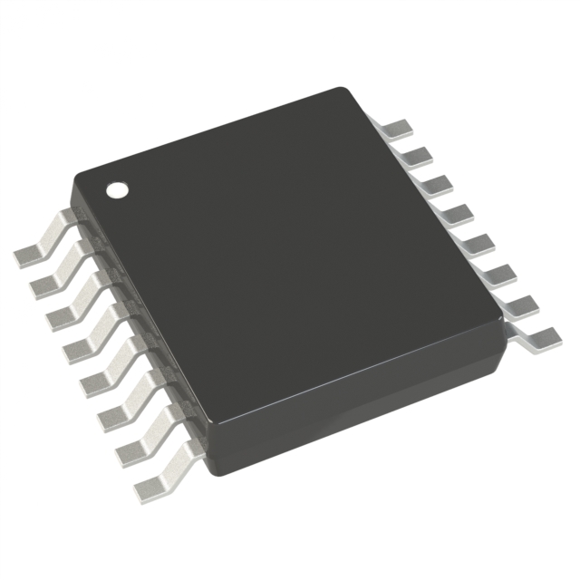
Package
The AD7398BRU comes in a small outline integrated circuit (SOIC) package.
Essence
The essence of the AD7398BRU lies in its ability to convert digital signals into accurate analog voltage outputs.
Packaging/Quantity
The AD7398BRU is typically packaged in reels and is available in quantities of 2500 units per reel.
Specifications
- Resolution: 12 bits
- Supply Voltage: 2.7V to 5.5V
- Output Voltage Range: 0V to Vref
- Operating Temperature Range: -40°C to +85°C
- Package Type: SOIC
Detailed Pin Configuration
The AD7398BRU has the following pin configuration:
- VDD: Power supply input
- GND: Ground reference
- DIN: Digital input for data
- CS: Chip select input
- SCLK: Serial clock input
- LDAC: Load DAC input
- REFOUT: Reference voltage output
- VOUT: Analog voltage output
Functional Features
- Serial interface: The AD7398BRU utilizes a serial interface for easy integration with microcontrollers or other digital systems.
- Power-down mode: It has a power-down mode to conserve energy when not in use.
- Internal reference: The DAC includes an internal voltage reference, eliminating the need for an external reference source.
Advantages and Disadvantages
Advantages
- High resolution provides accurate analog outputs.
- Low power consumption makes it suitable for battery-powered devices.
- Fast settling time enables quick response in dynamic applications.
- Wide temperature range allows for operation in various environments.
Disadvantages
- Limited output voltage range (0V to Vref).
- Requires an external voltage reference for precise output.
Working Principles
The AD7398BRU operates by converting digital input data into an analog voltage output. It utilizes a serial interface to receive digital data, which is then converted using an internal digital-to-analog conversion algorithm. The resulting analog voltage is available at the VOUT pin.
Detailed Application Field Plans
The AD7398BRU finds applications in various fields, including:
- Industrial automation: Used for controlling analog devices in industrial processes.
- Test and measurement equipment: Provides accurate analog signals for testing and measuring purposes.
- Audio equipment: Used in audio systems for generating analog audio signals.
- Communication systems: Enables analog signal generation in communication devices.
Detailed and Complete Alternative Models
- AD5628: 12-bit DAC with similar specifications and package type.
- MCP4921: 12-bit DAC with SPI interface and similar characteristics.
- MAX5216: 12-bit DAC with low power consumption and wide temperature range.
These alternative models offer similar functionality and can be considered as alternatives to the AD7398BRU.
Word count: 455 words
10 domande e risposte comuni relative all'applicazione di AD7398BRU nelle soluzioni tecniche
Sure! Here are 10 common questions and answers related to the application of AD7398BRU in technical solutions:
Q: What is the AD7398BRU? A: The AD7398BRU is a digital-to-analog converter (DAC) chip manufactured by Analog Devices.
Q: What is the resolution of the AD7398BRU? A: The AD7398BRU has a resolution of 12 bits, allowing it to convert digital signals into analog voltages with high precision.
Q: What is the output voltage range of the AD7398BRU? A: The AD7398BRU has a bipolar output voltage range of ±10V, which can be adjusted using external reference voltages.
Q: How does the AD7398BRU communicate with a microcontroller or other digital devices? A: The AD7398BRU uses a serial interface, such as SPI (Serial Peripheral Interface), to communicate with external devices.
Q: Can the AD7398BRU operate on a single power supply? A: Yes, the AD7398BRU can operate on a single power supply ranging from +2.7V to +5.5V.
Q: What is the settling time of the AD7398BRU? A: The settling time of the AD7398BRU is typically 1.5μs, ensuring fast response times for changing analog outputs.
Q: Does the AD7398BRU have any built-in reference voltage? A: No, the AD7398BRU requires an external reference voltage for accurate conversion. It supports both internal and external references.
Q: Can the AD7398BRU drive capacitive loads directly? A: Yes, the AD7398BRU is designed to drive capacitive loads up to 100pF without requiring any external components.
Q: What is the power consumption of the AD7398BRU? A: The power consumption of the AD7398BRU depends on the operating conditions but typically ranges from 1mW to 5mW.
Q: Can multiple AD7398BRU chips be cascaded together? A: Yes, multiple AD7398BRU chips can be cascaded together to increase the number of output channels or achieve higher resolution.
Please note that these answers are general and may vary depending on specific application requirements and datasheet specifications.