

Vedi le specifiche per i dettagli del prodotto.
AD5551BR
Product Overview
Category
AD5551BR belongs to the category of integrated circuits (ICs).
Use
The AD5551BR is primarily used for digital-to-analog conversion in various electronic systems.
Characteristics
- High precision and accuracy
- Low power consumption
- Wide operating voltage range
- Fast settling time
- Small form factor
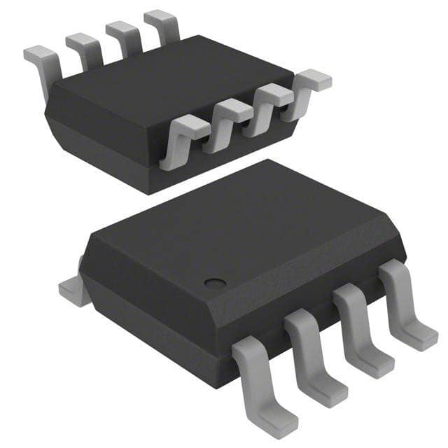
Package
AD5551BR is available in a small outline package (SOP) with a specified pin configuration.
Essence
The essence of AD5551BR lies in its ability to convert digital signals into analog voltages with high precision and accuracy.
Packaging/Quantity
AD5551BR is typically packaged in reels or tubes, with each reel/tube containing a specific quantity of ICs.
Specifications
- Resolution: 16 bits
- Supply Voltage Range: 2.7V to 5.5V
- Operating Temperature Range: -40°C to +85°C
- Output Voltage Range: 0V to Vref
- Conversion Rate: Up to 1 MSPS (Mega Samples Per Second)
- Power Consumption: Low power mode available
Detailed Pin Configuration
The AD5551BR has a total of 20 pins, each serving a specific function. The detailed pin configuration is as follows:
- VDD: Positive power supply
- GND: Ground reference
- REFOUT: Reference output voltage
- AGND: Analog ground reference
- AIN: Analog input voltage
- AVDD: Analog power supply
- DVDD: Digital power supply
- DIN: Serial data input
- SCLK: Serial clock input
- SYNC: Synchronization input
- LDAC: Load DAC input
- RESET: Reset input
- VOUT: Analog output voltage 14-20. NC: No connection
Functional Features
- High-resolution digital-to-analog conversion
- Serial interface for easy integration with microcontrollers
- On-chip reference voltage generator
- Power-down mode for reduced power consumption
- Flexible synchronization options
Advantages and Disadvantages
Advantages
- High precision and accuracy in analog voltage generation
- Wide operating voltage range allows for compatibility with various systems
- Fast settling time ensures quick response to input changes
- Low power consumption for energy-efficient applications
- Small form factor enables compact system designs
Disadvantages
- Limited output voltage range compared to some other DACs
- Higher cost compared to lower-resolution DACs
Working Principles
AD5551BR utilizes a digital-to-analog conversion technique known as pulse-width modulation (PWM). The digital input signal is converted into a series of pulses, where the width of each pulse corresponds to the desired analog voltage level. These pulses are then filtered to obtain a smooth analog output voltage.
Detailed Application Field Plans
AD5551BR finds applications in various fields, including but not limited to: - Audio equipment - Industrial automation - Test and measurement instruments - Communication systems - Medical devices
Alternative Models
For those seeking alternative models, the following options provide similar functionality to AD5551BR: - AD5552BR: 14-bit resolution, lower cost - AD5553BR: 18-bit resolution, higher precision - AD5554BR: 12-bit resolution, faster conversion rate
These alternatives cater to different requirements and can be chosen based on specific application needs.
Word count: 443 words
10 domande e risposte comuni relative all'applicazione di AD5551BR nelle soluzioni tecniche
Sure! Here are 10 common questions and answers related to the application of AD5551BR in technical solutions:
Q1: What is the AD5551BR? A1: The AD5551BR is a high-performance, low-power, 16-bit digital-to-analog converter (DAC) that can be used in various technical applications.
Q2: What is the operating voltage range of the AD5551BR? A2: The AD5551BR operates from a single power supply voltage range of 2.7 V to 5.5 V.
Q3: What is the resolution of the AD5551BR? A3: The AD5551BR has a resolution of 16 bits, allowing for precise analog output.
Q4: What is the typical settling time of the AD5551BR? A4: The typical settling time of the AD5551BR is 8 μs, ensuring fast and accurate output response.
Q5: Can the AD5551BR be used in industrial control systems? A5: Yes, the AD5551BR is suitable for use in industrial control systems due to its high precision and reliability.
Q6: Does the AD5551BR support serial communication interfaces? A6: Yes, the AD5551BR supports both SPI (Serial Peripheral Interface) and I2C (Inter-Integrated Circuit) communication interfaces.
Q7: What is the maximum output voltage range of the AD5551BR? A7: The AD5551BR has a maximum output voltage range of 0 V to VREF, where VREF is the reference voltage supplied to the DAC.
Q8: Can the AD5551BR be used in battery-powered applications? A8: Yes, the AD5551BR's low-power consumption makes it suitable for battery-powered applications, helping to conserve energy.
Q9: Does the AD5551BR have built-in power-on reset circuitry? A9: Yes, the AD5551BR includes a power-on reset circuit that ensures proper initialization upon power-up.
Q10: Is the AD5551BR available in a small package size? A10: Yes, the AD5551BR is available in a compact 16-lead TSSOP (Thin Shrink Small Outline Package) for space-constrained applications.
Please note that these answers are general and may vary depending on specific application requirements.